Features: • Supports bus operation up to 225 MHz
• Available speed grades are 225, 200 and 166 MHz
• Registered inputs and outputs for pipelined operation
• Optimal for performance (Double-Cycle deselect)
- Depth expansion without wait state
• 3.3V 5% and +10% core power supply (VDD)
• 2.5V / 3.3V I/O operation
• Fast clock-to-output times
- 2.8 ns (for 225-MHz device)
- 3.0 ns (for 200-MHz device)
- 3.5 ns (for 166-MHz device)
• Provide high-performance 3-1-1-1 access rate
• User-selectable burst counter supporting Intel®Pentium® interleaved or linear burst sequences
• Separate processor and controller address strobes
• Synchronous self-timed writes
• Asynchronous output enable
• Offered in JEDEC-standard 100-pin TQFP, 119-ball BGAand 165-Ball fBGA packages
• IEEE 1149.1 JTAG-Compatible Boundary Scan
• "ZZ" Sleep Mode Option
Pinout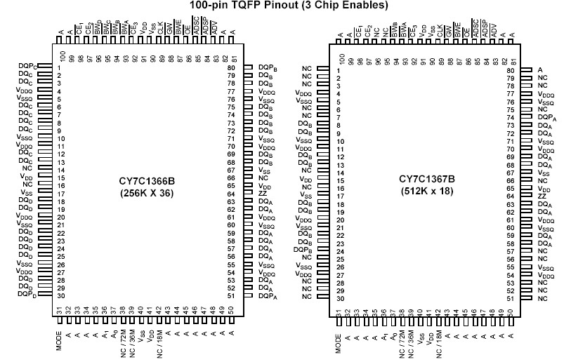 Specifications
(Above which the useful life may be impaired. For user guidelines,not tested.)
Storage Temperature .................................65 to +150
Ambient Temperature with
Power Applied.............................................55 to +125
Supply Voltage on VDD Relative to GND........0.5V to +4.6V
DC Voltage Applied to Outputs
in three-state ....................................0.5V to VDDQ + 0.5V
DC Input Voltage..................................0.5V to VDD + 0.5V
Current into Outputs (LOW)........................................20 mA
Static Discharge Voltage...........................................>2001V
(per MIL-STD-883, Method 3015)
Latch-up Current.....................................................>200 mA
DescriptionThe CY7C1366B/CY7C1367B SRAM integrates 262,144 x 36and 524,288 x 18 SRAM cells with advanced synchronousperipheral circuitry and a two-bit counter for internal burstoperation. All synchronous inputs are gated by registerscontrolled by a positive-edge-triggered Clock Input (CLK). Thesynchronous inputs of CY7C1366B/CY7C1367B include all addresses, all data inputs,address-pipelining Chip Enable (CE1), depth-expansion ChipEnables (CE2and CE3[2]), Burst Control inputs (ADSC , ADSP,and ADV), Write Enables ( BW X, and BWE ), and Global Write( GW). Asynchronous inputs include the Output Enable (OE)and the ZZ pin.
Addresses and chip of CY7C1366B/CY7C1367B enables are registered at rising edge ofclock when either Address Strobe Processor (ADSP) or Address Strobe Controller (ADSC) are active. Subsequentburst addresses can be internally generated as controlled by
the Advance pin (ADV).
Address, data inputs, and write controls CY7C1366B/CY7C1367B are registered on-chipto initiate a self-timed Write cycle.This part supports Byte Writeoperations (see Pin Descriptions and Truth Table for furtherdetails). Write cycles can be one to four bytes wide ascontrolled by the byte write control inputs. GW active LOWcauses all bytes to be written. This device incorporates anadditional pipelined enable register CY7C1366B/CY7C1367B which delays turning offthe output buffers an additional cycle when a deselect isexecuted.This feature allows depth expansion without penalizingsystem performance.
The CY7C1366B/CY7C1367B operates from a +3.3V corepower supply while all outputs operate with a +3.3V or a +2.5Vsupply. All inputs and outputs are JEDEC-standardJESD8-5-compatible.

 CY7C1367B Data Sheet


