Features: •Pin-compatible and functionally equivalent to ZBT™
•Supports 250-MHz bus operations with zero wait states
-Available speed grades are 250, 225, 200 and 167 MHz
•Internally self-time d output buffer cont rol to eliminate the need to use asynchronous OE
•Fully registered (inputs and outputs) for pipelined operation
•Byte Write capability
•Single 2.5V power supply
•Fast clock-to-output times
-2.6 ns (for 250-MHz device)
-2.8 ns (for 225-MHz device)
-3.0 ns (for 200-MHz device)
-3.4 ns (for 167-MHz device)
•Clock Enable (CEN) pin to suspend operation
•Synchronous self-timed writes
•Available in 100 TQFP, 119 BGA, and 165 fBGA packages
•IEEE 1149.1 JTAG Boundary Scan
•Burst capability-linear or interleaved burst order
•"ZZ" Sleep Mode option and Stop Clock optionPinout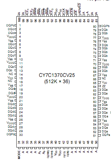 Specifications
Storage Temperature ........................................................ -65 to +150
Ambient Temperature with
Power Applied.....................................................................-55 to +125
Supply Voltage on VDD Relative to GND................................-0.5V to +4.6V
DC to Outputs in Tri-State...........................................-0.5V to VDDQ +0.5V
DC Input Voltage...........................................................-0.5V to VDD +0.5V
Current into Outputs(LOW) ................................................................20mA
Static Discharge Voltage ................................................................>2001V
(per MIL-STD-883,Method 3015)
Latch-up Current............................................................................>200mA
DescriptionThe CY7C1370CV25 and CY7C1372CV25 are 2.5V, 512K x36 and 1M x 18 Synchronous pipelined burst SRAMs with NoBus Latency™ (NoBL) logic, respectively. They are designed to support unlimited true back-to-back Read/Write operations with no wait states. The CY7C1370CV25 and CY7C1372CV25 are equipped with the advanced (NoBL) logic required to enable consecutive Read/Write operations with data being transferred on every clock cycle. This feature dramatically improves the thr oughput of data in systems that require frequent Write/Read transitions. The CY7C1370CV25 and CY7C1372CV25 are pin compatible and functionally equivalent to ZBT devices.
All synchronous inputs of CY7C1370CV25 and CY7C1372CV25 pass through input registers controlled by the rising edge of the clock. All data outputs pass through output registers controlled by t
he rising edge of the clock. The clock input of CY7C1370CV25 and CY7C1372CV25 is qualified by the Clock Enable (CEN) signal, which when deasserted suspends operation and extends the previous clock cycle.
Write operations are controlled by the Byte Write Selects (BW aBW d for CY7C1370CV25 and BWaBWb for CY7C1372CV25) and a Write Enable (WE) input. All writes areconducted with on-chip synchronous self-timed write circuitry. Three synchronous Chip Enables (CE1, CE2, CE3) and anasynchronous Output Enable (OE)CY7C1370CV25 and CY7C1372CV25 provide for easy bankselection and output three-state control. In order to avoid buscontention, the output drivers are synchronously three-stated during the data portion of a write sequence.

 CY7C1370CV25 Data Sheet


