Features: •Supports bus operation up to 250 MHz
•Available speed grades are 250, 200 and 167 MHz
•Registered inputs and outputs for pipelined operation
•3.3V core power supply
•2.5V / 3.3V I/O operation
•Fast clock-to-output times
-2.6 ns (for 250-MHz device)
-3.0 ns (for 200-MHz device)
-3.4 ns (for 167-MHz device)
•Provide high-performance 3-1-1-1 access rate
•User-selectable burst counter supporting Intel® Pentium interleaved or linear burst sequences
•Separate processor and controller address strobes
•Synchronous self-timed writes
•Asynchronous output enable
•Single Cycle Chip Deselect
•Offered in JEDEC-standard lead-free 100-pin TQFP, 119-ball BGA and 165-Ball fBGA packages
•IEEE 1149.1 JTAG-Compatible Boundary Scan
•"ZZ" Sleep Mode OptionPinout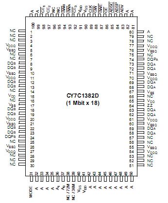 Specifications(Above which the useful life may be impaired. For user guide-lines, not tested.)
Storage Temperature ..............................65°C to +150°C
Ambient Temperature with
Power Applied...........................................55°C to +125°C
Supply Voltage on VDD Relative to GND..........0.3V to +4.6V
DC Voltage Applied to Outputs
in Tri-State...........................................0.5V to VDDQ + 0.5V
DC Input Voltage....................................0.5V to VDD + 0.5V
Current into Outputs (LOW).........................................20 mA
Static Discharge Voltage........................................... >2001V
(per MIL-STD-883, Method 3015)
Latch-up Current..................................................... >200 mADescriptionThe CY7C1380D/CY7C1382D SRAM integrates 524,288 x 36 and 1,048,576 x 18 SRAM cells with advanced synchronous peripheral circuitry and a two-bit counter for internal burst operation. All synchronous inputs of CY7C1380D/CY7C1382D are gated by registers controlled by a positive-edge-triggered Clock Input (CLK). The synchronous inputs include all addresses, all data inputs,address-pipelining Chip Enable (CE</a>1), depth-expansion Chip Enables (CE</a>2 and CE</a>3[2]), Burst Control inputs (ADSC</a>, ADSP</a>,and ADV</a>), Write Enables (BW</a>X, and BWE</a>), and Global Write(GW</a>). Asynchronous inputs include the Output Enable (OE</a>) and the ZZ pin.
Addresses and chip of CY7C1380D/CY7C1382D enables are registered at rising edge of clock when either Address Strobe Processor (ADSP</a>) or Address Strobe Controller (ADSC</a>) are active. Subsequent burst addresses of CY7C1380D/CY7C1382D can be internally generated as controlled by the Advance pin (ADV</a>).
Address, data inputs, and write controls are registered on-chip to initiate a self-timed Write cycle.This part supports Byte Write operations (see Pin Descriptions and Truth Table for further details). Write cycles of CY7C1380D/CY7C1382D can be one to two or four bytes wide as controlled by the byte write control inputs. GW</a>
when active LOW causes all bytes to be written.
The CY7C1380D/CY7C1382D operates from a +3.3V core power supply while all outputs may operate with either a +2.5 or +3.3V supply. All inputs and outputs are JEDEC-standard JESD8-5-compatible.

 CY7C1382D Data Sheet


