CY7C1399D

Features: • Pin- and function-compatible with CY7C1399B• Single 3.3V power supply• Ideal for low-voltage cache memory applications• High speed- tAA = 8 ns• Low active power- ICC = 60 mA @ 10 ns• Low CMOS standby power- ISB2 = 1.2 mA ( L Version only)• Dat...

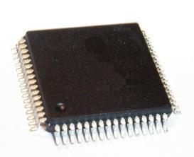
product image

CY7C1399D Picture
SeekIC No. : 004320098 Detail

CY7C1399D: Features: • Pin- and function-compatible with CY7C1399B• Single 3.3V power supply• Ideal for low-voltage cache memory applications• High speed- tAA = 8 ns• Low active p...

floor Price/Ceiling Price

Part Number:
CY7C1399D
Supply Ability:
5000

Price Break

  • Qty
  • 1~5000
  • Unit Price
  • Negotiable
  • Processing time
  • 15 Days
Total Cost: $ 0.00

SeekIC Buyer Protection PLUS - newly updated for 2013!

  • Escrow Protection.
  • Guaranteed refunds.
  • Secure payments.
  • Learn more >>

Month Sales

268 Transactions

Rating

evaluate  (4.8 stars)

Upload time: 2024/5/4

Payment Methods

All payment methods are secure and covered by SeekIC Buyer Protection PLUS.

Notice: When you place an order, your payment is made to SeekIC and not to your seller. SeekIC only pays the seller after confirming you have received your order. We will also never share your payment details with your seller.
Product Details

Description


Features:

• Pin- and function-compatible with CY7C1399B
• Single 3.3V power supply
• Ideal for low-voltage cache memory applications
• High speed
- tAA = 8 ns
• Low active power
- ICC = 60 mA @ 10 ns
• Low CMOS standby power
- ISB2 = 1.2 mA ("L" Version only)
• Data Retention at 2.0V
• Available in 28-SOJ and 28-TSOP I Pb-Free packages


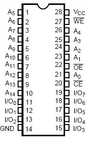
Pinout

  Connection Diagram


Specifications

(Above which the useful life may be impaired. For user guidelines,
not tested.)
Storage Temperature .................................65°C to +150°C
Ambient Temperature with
Power Applied.............................................55°C to +125°C
Supply Voltage on VCC to Relative GND[2] .... 0.5V to +4.6V
DC Voltage Applied to Outputs
in High-Z State[2] ...................................0.5V to VCC + 0.5V
DC Input Voltage[2] ................................0.5V to VCC + 0.5V
Output Current into Outputs (LOW)............................. 20 mA
Static Discharge Voltage............................................ > 2001V
(per MIL-STD-883, Method 3015)..
Latch-up Current...................................................... > 200 mA


Description

The CY7C1399D is a high-performance 3.3V CMOS Static RAM organized as 32,768 words by 8 bits. Easy memory expansion is provided by an active LOW Chip Enable (CE) and active LOW Output Enable (OE) and tri-state drivers. The device has an automatic power-down feature, reducing the power consumption when deselected.

An active LOW Write Enable signal (WE) of CY7C1399D controls the writing/reading operation of the memory. When CE and WE inputs are both LOW, data on the eight data input/output pins (I/O0 through I/O7) is written into the memory location addressed by the address present on the address pins (A0 through A14). Reading the device is accomplished by selecting the device and enabling the outputs, CE and OE active LOW, while WE remains inactive or HIGH. Under these conditions, the contents of the location addressed by the information o address pins is present on the eight data input/output pins.

The input/output pins of CY7C1399D remain in a high-impedance state unless the chip is selected, outputs are enabled, and Write Enable (WE) is HIGH. The CY7C1399D is available in 28-pin standard 300-mil-wide SOJ and TSOP Type I Pb-Free packages.


Customers Who Bought This Item Also Bought

Margin,quality,low-cost products with low minimum orders. Secure your online payments with SeekIC Buyer Protection.
Isolators
Integrated Circuits (ICs)
Fans, Thermal Management
Motors, Solenoids, Driver Boards/Modules
Boxes, Enclosures, Racks
View more