Features: •Supports bus operation up to 250 MHz
•Available speed grades are 250, 200,167 MHz
•Registered inputs and outputs for pipelined operation
•3.3V core power supply
•2.5V / 3.3V I/O operation
•Fast clock-to-output times
-3.0 ns (for 250-MHz device)
-3.0 ns (for 200-MHz device)
-3.4 ns (for 167-MHz device)
•Provide high-performance 3-1-1-1 access rate
•User-selectable burst counter supporting Intel®Pentium®interleaved or linear burst sequences
•Separate processor and controller address strobes
•Synchronous self-timed writes
•Asynchronous output enable
•Single Cycle Chip Deselect
•CY7C1480V33 and CY7C1482V33 offered in JEDEC-standard lead-free 100-pin TQFP, 165-Ball fBGA packages. CY7C1486V33 available in 209-Ball BGA packages
•IEEE 1149.1 JTAG-Compatible Boundary Scan
•"ZZ" Sleep Mode OptionPinout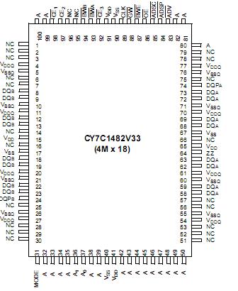 Specifications(Above which the useful life may be impaired. For user guide-lines, not tested.)
Storage Temperature ..............................65°C to +150°C
Ambient Temperature with
Power Applied.........................................55°C to +125°C
Supply Voltage on VDD Relative to GND........0.3V to +4.6V
DC Voltage Applied to Outputs
in Tri-State..........................................0.5V to VDDQ + 0.5V
DC Input Voltage...................................0.5V to VDD + 0.5V
Current into Outputs (LOW).........................................20 mA
Static Discharge Voltage........................................... >2001V
(per MIL-STD-883, Method 3015)
Latch-up Current..................................................... >200 mADescriptionThe CY7C1480V33/CY7C1482V33/CY7C1486V33 SRAM integrates 2,097,152 x 36/4,194,304 x 18,1,048,576 × 72 SRAM cells with advanced synchronous peripheral circuitry and a two-bit counter for internal burst operation. All synchronous inputs of CY7C1480V33/CY7C1482V33/CY7C1486V33 are gated by registers controlled by a positive-edge-triggered Clock Input (CLK). The synchronous inputs include all addresses, all data inputs, address-pipelining Chip Enable (CE</a>1), depth-expansion Chip Enables (CE</a>2 and CE</a>3), Burst Control inputs (ADSC</a>, ADSP</a>, and ADV</a>), Write Enables (BW</a>X, and BWE</a>), and Global Write (GW</a>).Asynchronous inputs include the Output Enable (OE</a>) and the ZZ pin.
Addresses and chip enables of CY7C1480V33/CY7C1482V33/CY7C1486V33 are registered at rising edge of clock when either Address Strobe Processor (ADSP</a>) or Address Strobe Controller (ADSC</a>) are active. Subsequent burst addresses can be internally generated as controlled by the Advance pin (ADV</a>).
Address, data inputs, and write controls of CY7C1480V33/CY7C1482V33/CY7C1486V33 are registered on-chip to initiate a self-timed Write cycle.This part supports Byte Write operations (see Pin Descriptions and Truth Table for further details). Write cycles can be one to two or four bytes wide as controlled by the byte write control inputs. GW</a> when active LOW causes all bytes to be written.
The CY7C1480V33/CY7C1482V33/CY7C1486V33 operates from a +3.3V core power supply while all outputs may operate with either a +2.5 or +3.3V supply. All inputs and outputs are JEDEC-standard JESD8-5-compatible.

 CY7C1482V33 Data Sheet


