CY7C408A

Features: • 64 x 8 and 64 x 9 first-in first-out (FIFO) buffer memory• 35-MHz shift in and shift out rates• Almost Full/Almost Empty and Half Full flags• Dual-port RAM architecture• Fast (50-ns) bubble-through• Independent asynchronous inputs and outputs• ...

product image

CY7C408A Picture
SeekIC No. : 004320330 Detail

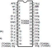
CY7C408A: Features: • 64 x 8 and 64 x 9 first-in first-out (FIFO) buffer memory• 35-MHz shift in and shift out rates• Almost Full/Almost Empty and Half Full flags• Dual-port RAM archit...

floor Price/Ceiling Price

Part Number:
CY7C408A
Supply Ability:
5000

Price Break

  • Qty
  • 1~5000
  • Unit Price
  • Negotiable
  • Processing time
  • 15 Days
Total Cost: $ 0.00

SeekIC Buyer Protection PLUS - newly updated for 2013!

  • Escrow Protection.
  • Guaranteed refunds.
  • Secure payments.
  • Learn more >>

Month Sales

268 Transactions

Rating

evaluate  (4.8 stars)

Upload time: 2024/4/30

Payment Methods

All payment methods are secure and covered by SeekIC Buyer Protection PLUS.

Notice: When you place an order, your payment is made to SeekIC and not to your seller. SeekIC only pays the seller after confirming you have received your order. We will also never share your payment details with your seller.
Product Details

Description


Features:

• 64 x 8 and 64 x 9 first-in first-out (FIFO) buffer memory
• 35-MHz shift in and shift out rates
• Almost Full/Almost Empty and Half Full flags
• Dual-port RAM architecture
• Fast (50-ns) bubble-through
• Independent asynchronous inputs and outputs
• Output enable (CY7C408A)
• Expandable in word width and FIFO depth
• 5V ± 10% supply
• TTL complete
• Capable of withstanding greater than 2001V electrostatic discharge voltage
• 300-mil, 28-pin DIP


Pinout

  Connection Diagram


Specifications

(Above which the useful life may be impaired. For user guidelines,not tested.)
Storage Temperature ..................................... -65°C to +150°C
Ambient Temperature with
Power Applied.................................................. -55°C to +125°C
Supply Voltage to Ground Potential .....................-0.5V to +7.0V
DC Voltage Applied to Outputs
in High Z State (7C408A).......................................-0.5V to +7.0V
DC Input Voltage ..................................................-3.0V to +7.0V
Power Dissipation............................................................... 1.0W
Output Current, into Outputs (Low) ................................. 20 mA
Static Discharge Voltage ............................................... >2001V
(per MIL-STD-883, Method 3015)


Description

 The CY7C408A and CY7C409A are 64-word deep by 8- or9-bit wide first-in first-out (FIFO) buffer memories. In addition to the industry-standard handshaking signals, almost full/almost empty (AFE) and half-full (HF) flags are provided.

AFE is HIGH when the FIFO CY7C408A and CY7C409A is almost full or almost empty, otherwise AFE is LOW. HF is HIGH when the FIFO is half full, otherwise HF is LOW.

The CY7C408A has an output enable (OE) function. The memory accepts 8- or 9-bit parallel words as its inputs (DI0 DI8) under the control of the shift in (SI) input when the input ready (IR) control signal is HIGH. The data is output, in the same order as it was stored on the DO0 DO8 output pins of CY7C408A and CY7C409A under the control of the shift out (SO) input when the output ready (OR) control signal is HIGH. If the FIFO is full (IR LOW), pulses at the SI input are ignored; if the FIFO is empty (OR LOW), pulses at the SO input are ignored.

The IR and OR signals CY7C408A and CY7C409A are also used to connect the FIFOs in parallel to make a wider word or in series to make a deeper buffer, or both.

Parallel expansion of CY7C408A and CY7C409A for wider words is implemented by logically ANDing the IR an OR outputs (respectively) of the individual FIFOs together (Figure 5). The AND operation insures that all of the FIFOs are either ready to accept more data (IR HIGH) or ready to output data (OR HIGH) and thus compensate for variations in propagation delay times between devices.

Serial expansion (cascading)CY7C408A and CY7C409A for deeper buffer memories is accomplished by connecting data outputs of the FIFO closet to the data source (upstream device) to the data inputs of the following (downstream) FIFO (Figure 4). In addition, to insure proper operation, the SO signal of the upstream FIFO CY7C408A and CY7C409A must be connected to the OR output of the upstream FIFO. In this serial expansion configuration, the IR and OR signals are used to pass data through the FIFOs.

Reading and writing operations of CY7C408A and CY7C409A are completely asynchronous, allowing the FIFO to be used as a buffer between two digital machines of widely differing operating frequencies. The high shift in and shift out rates of these FIFOs, and their throughput rate due to the fast bubblethrough time, which is due to their dual-port RAM architecture, make CY7C408A and CY7C409A ideal for high-speed communications and controllers.


Customers Who Bought This Item Also Bought

Margin,quality,low-cost products with low minimum orders. Secure your online payments with SeekIC Buyer Protection.
Crystals and Oscillators
Semiconductor Modules
Industrial Controls, Meters
Inductors, Coils, Chokes
Resistors
Fans, Thermal Management
View more