Features: • High-speed, low-power, first-in first-out (FIFO)
memories
• 64 x 18 (CY7C4425)
• 256 x 18 (CY7C4205)
• 512 x 18 (CY7C4215)
• 1K x 18 (CY7C4225)
• 2K x 18 (CY7C4235)
• 4K x 18 (CY7C4245)
• High-speed 100-MHz operation (10 ns read/write cycle
time)
• Low power (ICC =45 mA)
• Fully asynchronous and simultaneous read and write
operation
• Empty, Full, Half Full, and Programmable Almost
Empty/Almost Full status flags
• TTL-compatible
• Retransmit function
• Output Enable (OE) pin
• Independent read and write enable pins
• Center power and ground for reduced noise
• Supports free-running 50% duty cycle clock inputs
• Width Expansion Capability
• Depth Expansion Capability
• Space saving 64-pin 10x10 TQFP, and 14x14 TQFP
• 68-pin PLCCPinout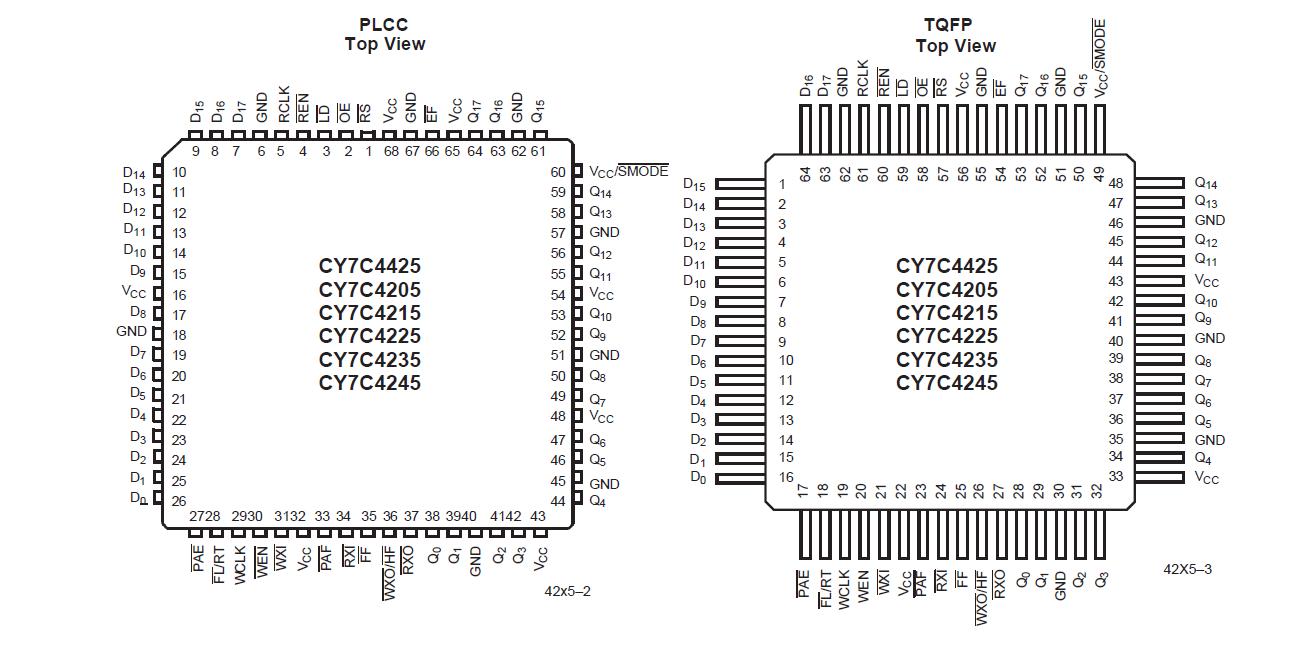 Specifications(Above which the useful life may be impaired. For user guidelines,
not tested.)
Storage Temperature .....................................................-65°C to +150°C
Ambient Temperature with
Power Applied.................................................................-55°C to +125°C
Supply Voltage to Ground Potential ...................................-0.5V to +7.0V
DC Voltage Applied to Outputs
in High Z State....................................................................-0.5V to +7.0V
DC Input Voltage ...............................................................-3.0V to +7.0V
Output Current into Outputs (LOW)................................................ 20 mA
Static Discharge Voltage .............................................................. >2001V
(per MIL-STD-883, Method 3015)
Latch-Up Current......................................................................... >200 mADescriptionThe CY7C42X5 are high-speed, low-power, first-in first-out (FIFO) memories with clocked read and write interfaces. The CY7C42X5 are 18 bits wide and are pin/functionally compatible to IDT722x5. The CY7C42X5 can be cascaded to increase FIFO depth. Programmable features include Almost Full/Almost Empty flags. The CY7C42X5 provide solutions for a wide variety of data buffering needs, including high-speed data acquisition, multiprocessor interfaces, and communications buffering.
The CY7C42X5 have 18-bit input and output ports that are controlled by separate clock and enable signals. The input port is controlled by a free-running clock (WCLK) and a write enable pin (WEN).
When WEN is asserted, data is written into the FIFO of the CY7C42X5 on the rising edge of the WCLK signal. While WEN is held active, data is continually written into the FIFO on each cycle. The output port is controlled in a similar manner by a free-running read clock (RCLK) and a read enable pin (REN). In addition, the CY7C42X5 have an output enable pin (OE). The read and write clocks may be tied together for single-clock operation or the two clocks may be run independently for asynchronous read/write applications. Clock frequencies up to 100 MHz are achievable.
Retransmit and Synchronous Almost Full/Almost Empty flag features are available on the CY7C42X5.
Depth expansion of CY7C42X5 is possible using the cascade input (WXI, RXI), cascade output (WXO, RXO), and First Load (FL) pins. The WXO and RXO pins are connected to the WXI and RXI pins of the next device, and the WXO and RXO pins of the last device should be connected to the WXI and RXI pins of the first device. The FL pin of the first device is tied to VSS and the FL pin of all the remaining devices should be tied to VCC.
The CY7C42X5 provides five status pins. These pins are decoded to determine one of five states: Empty, Almost Empty, Half Full, Almost Full, and Full (see Table 2). The Half Full flag shares the WXO pin. This flag is valid in the standalone and width-expansion configurations. In the depth expansion, this pin provides the expansion out (WXO) information that is used to signal the next FIFO when it will be activated.
The Empty and Full flags of the CY7C42X5 are synchronous, i.e., they change state relative to either the read clock (RCLK) or the write clock (WCLK). When entering or exiting the Empty states, the flag is updated exclusively by the RCLK. The flag denoting Full states is updated exclusively by WCLK. The synchronous flag architecture guarantees that the flags will remain valid from one clock cycle to the next. As mentioned previously, the Almost Empty/Almost Full flags become synchronous if the VCC/SMODE is tied to VSS. All configurations are fabricated using an advanced 0.65m N-Well CMOS technology. Input ESD protection is greater than 2001V, and latch-up is prevented by the use of guard rings.

 CY7C4245 Data Sheet


