Features: • High-speed, low-power, first-in first-out (FIFO) memories
• 64K * 9 (CY7C4282)
• 128K * 9 (CY7C4292)
• 0.5-micron CMOS for optimum speed/power
• High-speed, near-zero latency (true dual-ported memory cell), 100-MHz operation (10-ns read/write cycle times)
• Low power
-ICC=40 mA
-ISB = 2 mA
• Fully asynchronous and simultaneous read and write operation
• Empty, Full, and Programmable Almost Empty and Almost Full status flags
• TTL-compatible
• Retransmit function
• Output Enable (OE) pin
• Independent read and write enable pins
• Supports free-running 50% duty cycle clock inputs
• Width-Expansion Capability
• Depth-Expansion Capability through token-passing scheme (no external logic required)
• 64-pin 10 * 10 STQFPPinout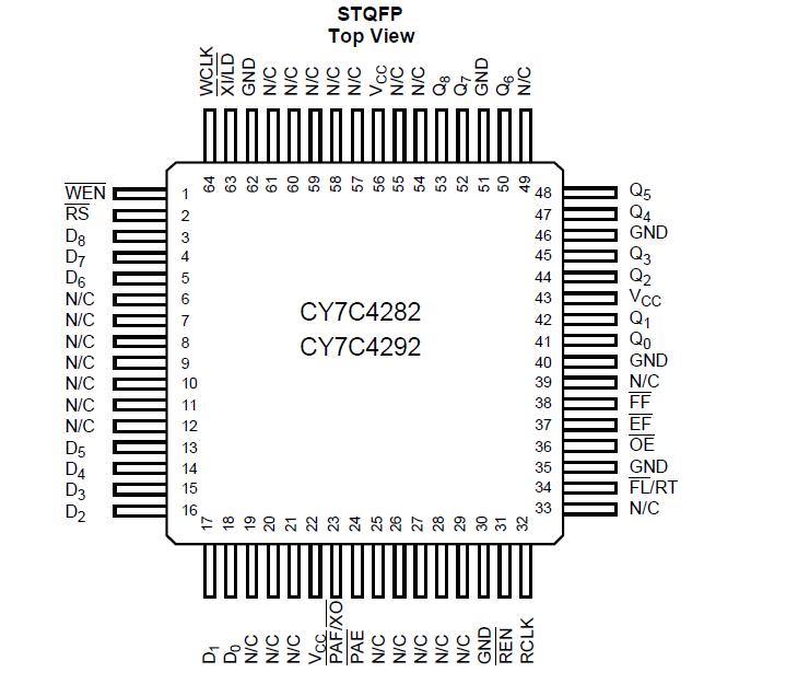 Specifications(Above which the useful life may be impaired. For user guidelines, not tested.)
Storage Temperature ..........................................−65°C to +150°C
Ambient Temperature with
Power Applied......................................................−55°C to +125°C
Supply Voltage to Ground Potential .........................−0.5V to +7.0V
DC Voltage Applied to Outputs
in High-Z State ...................................................−0.5V to VCC+0.5V
DC Input Voltage ..............................................−0.5V to VCC +0.5V
Output Current into Outputs (LOW)....................................... 20 mA
Static Discharge Voltage..................................................... > 2001V
(per MIL-STD-883, Method 3015)
Latch-up Current............................................................... > 200 mADescriptionThe CY7C4282/CY7C4292 are high-speed, low-power, FIFO memories with clocked read and write interfaces. All devices are nine bits wide. The CY7C4282/CY7C4292 can be cascaded to increase FIFO depth. Programmable features include Almost Full/Almost Empty flags. The CY7C4282/CY7C4292 provide solutions for a wide variety of data buffering needs, including high-speed data acquisition, multiprocessor interfaces, video and communications buffering.
The CY7C4282/CY7C4292 have 9-bit input and output ports that are controlled by separate clock and enable signals. The input port is controlled by a free-running clock (WCLK) and a write-enable pin (WEN).
Retransmit and Synchronous Almost Full/Almost Empty flag features are available on the CY7C4282/CY7C4292 . Depth expansion is possible using the cascade input (XI), cascade output (XO), and First Load (FL) pins. The XO pin is connected to the XI pin of the next device, and the XO pin of the last device should be connected to the XI pin of the first device. The FL pin of the first device is tied to VSS and the FL pin of all the remaining devices should be tied to VCC.
When WEN is asserted, data is written into the FIFO of the CY7C4282/CY7C4292 on the rising edge of the WCLK signal. While WEN is held active, data is continually written into the FIFO on each cycle. The output port is controlled in a similar manner by a free-running read clock (RCLK) and a read enable pin (REN). In addition, the CY7C4282/92 have an output enable pin (OE). The read and write clocks may be tied together for single-clock operation or the two clocks may be run independently for asynchronous read/write applications. Clock frequencies up to 100 MHz are achievable.

 CY7C4282 Data Sheet


