CY7C60113

Features: • enCoRe™ II Low Voltage (enCoRe II LV)- enhanced Component Reduction - Internal crystalless oscillator with support for optional external clock or external crystal or resonator. - Configurable IO for real-world interface without external components• Enhanced 8-bit mic...

product image

CY7C60113 Picture
SeekIC No. : 004320471 Detail

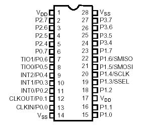
CY7C60113: Features: • enCoRe™ II Low Voltage (enCoRe II LV)- enhanced Component Reduction - Internal crystalless oscillator with support for optional external clock or external crystal or resonat...

floor Price/Ceiling Price

Part Number:
CY7C60113
Supply Ability:
5000

Price Break

  • Qty
  • 1~5000
  • Unit Price
  • Negotiable
  • Processing time
  • 15 Days
Total Cost: $ 0.00

SeekIC Buyer Protection PLUS - newly updated for 2013!

  • Escrow Protection.
  • Guaranteed refunds.
  • Secure payments.
  • Learn more >>

Month Sales

268 Transactions

Rating

evaluate  (4.8 stars)

Upload time: 2024/4/30

Payment Methods

All payment methods are secure and covered by SeekIC Buyer Protection PLUS.

Notice: When you place an order, your payment is made to SeekIC and not to your seller. SeekIC only pays the seller after confirming you have received your order. We will also never share your payment details with your seller.
Product Details

Description


Features:

• enCoRe™ II Low Voltage (enCoRe II LV)-"enhanced Component Reduction"
    - Internal crystalless oscillator with support for optional external clock or external crystal or resonator.
    - Configurable IO for real-world interface without external components
• Enhanced 8-bit microcontroller
    - Harvard architecture
    - M8C CPU speed can be up to 12 MHz or sourced by an external crystal, resonator, or clock signal
• Internal memory
    - 256 bytes of RAM
    - 8 Kbytes of Flash including EEROM emulation
• Low power consumption
    - Typically 2.25 mA at 3 MHz
    - 5 µA sleep
• In-system reprogrammability
    - Allows easy firmware update
• General-purpose I/O ports
    - Up to 36 General Purpose I/O (GPIO) pins
    - High current drive on GPIO pins. Configurable 8- or 50- mA/pin current sink on designated pins
    - Each GPIO port supports high-impedance inputs, configurable pull-up, open drain output, CMOS/TTL inputs, and CMOS output
    - Maskable interrupts on all I/O pins
• SPI serial communication
    - Master or slave operation
    - Configurable up to 2-Mbit/second transfers.
    - Supports half duplex single data line mode for optical sensors
• 2-channel 8-bit or 1-channel 16-bit capture timer registers. Capture timer registers store both rising and falling edge times
    - Two registers each for two input pins
    - Separate registers for rising and falling edge capture
    - Simplifies interface to RF inputs for wireless applications
• Internal low-power wake-up timer during suspend mode
    - Periodic wake-up with no external components
• Programmable Interval Timer interrupts
• Reduced RF emissions at 27 MHz and 96 MHz
• Watchdog timer (WDT)
• Low voltage detection with user-selectable threshold voltages
• Improved output drivers to reduce EMI
• Operating voltage from 2.7V to 3.6VDC
• Operating temperature from 070°C
• Available in 24/40-pin PDIP, 24-pin SOIC, 24-pin QSOP/SSOP, 28-pin SSOP and 48-pin SSOP.
• Advanced development tools based on Cypress PSoC® tools
• Industry-standard programmer support


Application

The CY7C601xx/CY7C602xx is targeted for the following applications:
• PC Wireless HID devices
    - Mice (optomechanical, optical, trackball)
    - Keyboards
    - Presenter tools
• Gaming
    - Joysticks
    - Gamepad
• General purpose wireless applications
    - Remote controls
    - Barcode scanners
    - POS terminal
    - Consumer electronics
    - Toys


Pinout

  Connection Diagram


Specifications

Storage Temperature .................................65°C to +150°C
Ambient Temperature with Power Applied ..... 0°C to +70°C
Supply Voltage on VCC Relative to VSS ......... 0.5V to +7.0V
DC Input Voltage................................ 0.5V to + VCC + 0.5V
DC Voltage Applied to Outputs in
High-Z State ....................................... 0.5V to + VCC + 0.5V
Maximum Total Sink Output Current into Port 0
and 1 and Pins............................................................. 70 mA
Maximum Total Source Output Current into GPIO Pins30 mA
Maximum On-chip Power Dissipation
on any GPIO Pin......................................................... 50 mW
Power Dissipation .................................................... 300 mW
Static Discharge Voltage ............................................. 2200V
Latch-up Current ...................................................... 200 mA


Description

An interrupt,CY7C60113 is posted when CY7C60113's  interrupt conditions occur. This results in the flip-flop in Figure 17 clocking in a '1'. The interrupt will remain posted until the interrupt is taken or until it is cleared by writing to the appropriate INT_CLRx register.

A posted interrupt is not pending unless it is enabled by setting its interrupt mask bit (in the appropriate INT_MSKx register). All pending interrupts of the CY7C60113 are processed by the Priority Encoder to determine the highest priority interrupt which will be taken by the M8C if the Global Interrupt Enable bit is set in the CPU_F register.

Disabling an interrupt by clearing CY7C60113's interrupt mask bit (in the INT_MSKx register) does not clear a posted interrupt, nor does it prevent an interrupt from being posted. It simply prevents a posted interrupt from becoming pending.

Nested interrupts can be accomplished by reenabling interrupts inside an interrupt service routine. To do this, set the IE bit in the Flag Register. A block diagram of the enCoRe II LV Interrupt Controller is shown in Figure 17.


Customers Who Bought This Item Also Bought

Margin,quality,low-cost products with low minimum orders. Secure your online payments with SeekIC Buyer Protection.
Connectors, Interconnects
Static Control, ESD, Clean Room Products
Transformers
Power Supplies - External/Internal (Off-Board)
Isolators
View more