Features: • Low-cost solution for low-speed applications such as mice, gamepads, keyboards, joystick and others
• USB Specification Compliance
-Conforms to USB Specification, Versions 1.1 and 2.0
-Conforms to USB HID Specification, Version 1.1
-Supports 1 device address and 3 data endpoints
-Integrated USB transceiver
• 8-bit RISC microcontroller
-Harvard architecture
-6-MHz external ceramic resonator
-12-MHz internal CPU clock
• Internal memory
-256 bytes of RAM
-4 Kbytes of EPROM (CY7C63411, CY7C63511)
-6 Kbytes of EPROM (CY7C63412, CY7C63512, CY7C63612)
-8 Kbytes of EPROM (CY7C63413, CY7C63513, CY7C63613)
• Interface can auto-configure to operate as PS2 or USB
• I/O port
-The CY7634XX/5XX have 24 General Purpose I/O (GPIO) pins (Port 0 to 2) capable of sinking 7 mA per pin (typical)
-The CY7C636XX have 12 General-Purpose I/O (GPIO) pins (Port 0 to 2) capable of sinking 7 mA per pin (typical)
-The CY7C634XX/5XX have eight GPIO pins (Port 3) capable of sinking 12 mA per pin (typical) which can drive LEDs
-The CY7C636XX have four GPIO pins (Port 3) capable of sinking 12 mA per pin (typical) which can drive LEDs
-Higher current drive is available by connecting multiple GPIO pins together to drive a common output
-Each GPIO port can be configured as inputs with internal pull-ups or open drain outputs or traditional CMOS outputs
-The CY7C635XX has an additional eight I/O pins on a DAC port which has programmable current sink outputs
-Maskable interrupts on all I/O pins
• 12-bit free-running timer with one microsecond clock ticks
• Watch Dog Timer (WDT)
• Internal Power-On Reset (POR)
• Improved output drivers to reduce EMI
• Operating voltage from 4.0V to 5.5V DC
• Operating temperature from 0 to 70 degrees Celsius
• CY7C634XX available in 40-pin PDIP, 48-pin SSOP for production
• CY7C635XX available in 48-pin SSOP packages for production
• CY7C636XX available in 24-pin SOIC packages for production
• Industry-standard programmer supportPinout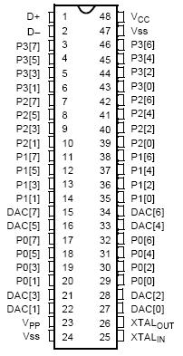 SpecificationsStorage Temperature ..................................................................................................65°C to +150°C
Ambient Temperature with Power Applied........................................................................0°C to +70°C
Supply Voltage on VCC relative to VSS..............................................................................0.5V to +7.0V
DC Input Voltage..................................................................................................... 0.5V to +VCC+0.5V
DC Voltage Applied to Outputs in High Z State ...................................................... 0.5V to + VCC+0.5V
Max. Output Current into Port 0,1,2,3 and DAC[1:0] Pins ............................................................. 60 mA
Max. Output Current into DAC[7:2] Pins......................................................................................... 10 mA
Power Dissipation ........................................................................................................................300 mW
Static Discharge Voltage ............................................................................................................. > 2000V
Latch-up Current ....................................................................................................................... > 200 mADescriptionThe CY7C634XX/5XX/6XX are 8-bit RISC One Time Programmable (OTP) microcontrollers. The instruction set has been optimized specifically for USB operations although, the microcontrollers,CY7C634XX/5XX/6XX can be used for a variety of non-USB embedded applications.
The CY7C634XX/5XX feature 32 General-Purpose I/O (GPIO) pins and the CY7C636XX features 16 General-Purpose I/O (GPIO) pins to support USB and other applications. The I/O pins are grouped into four ports (Port 0, 1, 2, and 3) where each port can be configured as inputs with internal pull-ups, open drain outputs, or traditional CMOS outputs. The CYC634XX/5XX have 24 GPIO pins (Ports 0, 1, and 2) and the CY7C636XX has 12 GPIO pins (Ports 0 and 1) that are rated at 7 mA typical sink current. The CYC634XX/5XX has 8 GPIO pins (Port 3) and the CY7C636XX has 4 GPIO pins (Port 3) which are rated at 12 mA typical sink current, which allows these pins to drive LEDs. Multiple GPIO pins can be connected together to drive a single output for more drive current capacity. Additionally, each I/O pin can be used to generate a GPIO interrupt to the microcontroller. Note the GPIO interrupts all share the same "GPIO" interrupt vector.
The CY7C635XX features an additional 8 I/O pins in the DAC port. Every DAC pin includes an integrated 14-Kohm pull-up resistor. When a "1" is written to a DAC I/O pin, the output current sink is disabled and the output pin is driven high by the internal pull-up resistor. When a "0" is written to a DAC I/O pin, the internal pull-up is disabled and the output pin provides the programmed amount of sink current. A DAC I/O pin can be used as an input with an internal pull-up by writing a "1" to the pin.
The sink current for each DAC I/O pin can be individually programmed to one of sixteen values using dedicated Isink registers. DAC bits [1:0] can be used as high current outputs with a programmable sink current range of 3.2 to 16 mA (typical). DAC bits [7:2] have a programmable current sink range of 0.2 to 1.0 mA (typical). Again, multiple DAC pins can be connected together to drive a single output that requires more sink current capacity. Each I/O pin can be used to generate a DAC interrupt to the microcontroller and the interrupt polarity for each DAC I/O pin is individually programmable. The DAC port interrupts share a separate "DAC" interrupt vector.
The Cypress microcontrollers,CY7C634XX/5XX/6XX use an external 6-MHz ceramic resonator to provide a reference to an internal clock generator. This clock generator reduces the clock-related noise emissions (EMI). The clock generator provides the 6- and 12-MHz clocks that remain internal to the microcontroller.
The CY7C64XX/5XX/6XX are offered with multiple EPROM options to maximize flexibility and minimize cost. The CY7C63411 and the CY7C63511 have 4 Kilobytes of EPROM. The CY7C63412, CY7C63512, and CY7C63612 have 6 Kbytes of EPROM. The CY7C63413, CY7C63513, and CY7C63613 have 8 Kbytes of EPROM.
The CY7C634XX/5XX/6XX include Power-on Reset logic, a Watch Dog Timer, a vectored interrupt controller, and a 12-bit free-running timer. The Power-On Reset (POR) logic detects when power is applied to the device, resets the logic to a known state, and begins executing instructions at EPROM address 0x0000h. The Watch Dog Timer can be used to ensure the firmware never gets stalled for more than approximately 8 ms. The firmware can get stalled for a variety of reasons, including errors in the code or a hardware failure such as waiting for an interrupt that never occurs. The firmware should clear the Watch Dog Timer periodically. If the Watch Dog Timer is not cleared for approximately 8 ms, the microcontroller will generate a hardware watch dog reset.
The microcontroller,CY7C634XX/5XX/6XX supports eight maskable interrupts in the vectored interrupt controller. Interrupt sources include the USB Bus- Reset, the 128-s and 1.024-ms outputs from the free-running timer, three USB endpoints, the DAC port, and the GPIO ports. The timer bits cause an interrupt (if enabled) when the bit toggles from LOW "0" to HIGH "1." The USB endpoints interrupt after either the USB host or the USB controller sends a packet to the USB. The DAC ports have an additional level of masking that allows the user to select which DAC inputs can cause a DAC interrupt. The GPIO ports also have a level of masking to select which GPIO inputs can cause a GPIO interrupt. For additional flexibility, the input transition polarity that causes an interrupt is programmable for each pin of the DAC port. Input transition polarity can be programmed for each GPIO port as part of the port
configuration. The interrupt polarity can be either rising edge ("0" to "1") or falling edge ("1" to "0").
The free-running 12-bit timerof CY7C634XX/5XX/6XX clocked at 1 MHz provides two interrupt sources as noted above (128-s and 1.024-ms). The timer can be used to measure the duration of an event under firmware control by reading the timer twice: once at the start of the event, and once after the event is complete. The difference between the two readings indicates the duration of the event measured in microseconds. The upper four bits of the timer are latched into an internal register when the firmware reads the lower eight bits. A read from the upper four bits actually reads data from the internal register, instead of the timer. This feature eliminates the need for firmware to attempt to compensate if the upper four bits happened to increment right after the lower 8 bits are read.
The CY7C634XX/5XX/6XX include an integrated USB serial interface engine (SIE) that supports the integrated peripherals. The hardware supports one USB device address with three endpoints. The SIE allows the USB host to communicate with the function integrated into the microcontroller.
Finally, the CY7C634XX/5XX/6XX support PS/2 operation. With appropriate firmware the D+ and D USB pins can also be used as PS/2 clock and data signals. Products utilizing these devices can be used for USB and/or PS/2 operation with appropriate firmware.

 CY7C63411 Data Sheet


