CY7C9915

Features: • All output pair skew <100 ps (typical)• Input Frequency Range: 3.75 MHz to 150 MHz• Output Frequency Range: 3.75 MHz to 150 MHz• User-selectable output functions - Selectable skew to 18 ns - Inverted and non-inverted - Operation at 1⁄2 and 1⁄4 inp...

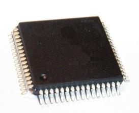
product image

CY7C9915 Picture
SeekIC No. : 004320541 Detail

CY7C9915: Features: • All output pair skew <100 ps (typical)• Input Frequency Range: 3.75 MHz to 150 MHz• Output Frequency Range: 3.75 MHz to 150 MHz• User-selectable output functio...

floor Price/Ceiling Price

Part Number:
CY7C9915
Supply Ability:
5000

Price Break

  • Qty
  • 1~5000
  • Unit Price
  • Negotiable
  • Processing time
  • 15 Days
Total Cost: $ 0.00

SeekIC Buyer Protection PLUS - newly updated for 2013!

  • Escrow Protection.
  • Guaranteed refunds.
  • Secure payments.
  • Learn more >>

Month Sales

268 Transactions

Rating

evaluate  (4.8 stars)

Upload time: 2024/4/24

Payment Methods

All payment methods are secure and covered by SeekIC Buyer Protection PLUS.

Notice: When you place an order, your payment is made to SeekIC and not to your seller. SeekIC only pays the seller after confirming you have received your order. We will also never share your payment details with your seller.
Product Details

Description


Features:

• All output pair skew <100 ps (typical)
• Input Frequency Range: 3.75 MHz to 150 MHz
• Output Frequency Range: 3.75 MHz to 150 MHz
• User-selectable output functions
   - Selectable skew to 18 ns
   - Inverted and non-inverted
   - Operation at 1⁄2 and 1⁄4 input frequency
   - Operation at 2x and 4x input frequency (input as low as 3.75 MHz)
• Zero input-to-output delay
• 3.3V power supply
• ± 3.0% Output Duty Cycle Distortion
• LVTTL outputs drive 50 terminated lines
• Low operating current
• 32-pin PLCC package
• Jitter < 100ps peak-to-peak (< 15 ps RMS)


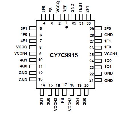
Pinout

  Connection Diagram


Specifications

Parameter
Description Condition
Min.
Max.
Unit
VDD
Supply Voltage Nonfunctional
0.5
4.6
VDC
VIN
Input Voltage REF Relative to VCC
0.5
4.6
VDC
VIN
Input Voltage Except REF Relative to VCC
0.5
VDD + 0.5
VDC
LUI
Latch-up Immunity Functional
300
mA
TS
Temperature, Storage Nonfunctional
65
+125
°C
TA
Temperature, Operating Ambient Commercial Temperature
0
+70
°C
TA
Temperature, Operating Ambient Industrial Temperature
-40
+85
°C
TJ
Junction Temperature Industrial Temperature
125
°C
ESDh
ESD Protection (Human Body Model)  
2000
V
MSL
Moisture Sensitivity Level  
MSL 3
Class
UL-94
Flammability Rating @ 1/8 in.
V0
Class
FIT
Failure in Time Manufacturing test
10
ppm
TPU
Power-up time for all VDDs to reach
minimum specified voltage (power ramps
must be monotonic)
 
0.05
500
ms
CIN
Input Capacitance[4] TA = 25°C, f = 1 MHz, VCC = 3.3V
-
10
pF
ZOUT
Output Impedance Low to High (Rising edge)
27
High to Low (Falling edge)
7


Description

The CY7C9915 RoboClock is a 150-MHz Low-voltage Programmable Skew Clock Buffer that offers user-selectable control over system clock functions. This multiple-output clock driver,CY7C9915 provides the system integrator with functions necessary to optimize the timing of high-performance computer systems. Eight individual drivers, arranged as four pairs of user-controllable outputs, can each drive terminated transmission lines with impedances as low as 50 while delivering minimal and specified output skews and full-swing logic levels (LVTTL).

Each output of the CY7C9915 can be hardwired to one of nine delay or function configurations. Delay increments of 0.42 to 1.6 ns are determined by the operating frequency with outputs able to skew up to ±6 time units from their nominal "zero" skew position. The completely integrated PLL allows external load and  ransmission line delay effects to be canceled. When this "zero delay" capability of the LVPSCB is combined with the selectable output skew functions, the user can create output-to-output delays of up to ±12 time units.

Divide-by-two and divide-by-four output functions of the CY7C9915 are provided for additional flexibility in designing complex clock systems. When combined with the internal PLL, these divide functions allow distribution of a low-frequency clock that can be multiplied by two or four at the clock destination. This facility minimizes clock distribution difficulty while allowing maximum system clock speed and flexibility.


Customers Who Bought This Item Also Bought

Margin,quality,low-cost products with low minimum orders. Secure your online payments with SeekIC Buyer Protection.
Line Protection, Backups
Memory Cards, Modules
Tapes, Adhesives
803
Circuit Protection
Inductors, Coils, Chokes
Audio Products
View more