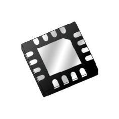
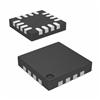
Features: CY8C24894 includes an XRES pin to support In-System Serial Programming (ISSP) and external reset control
Powerful Harvard Architecture Processor
❐ M8C Processor Speeds to 24 MHz
❐ Two 8x8 Multiply, 32-Bit Accumulate
❐ Low Power at High Speed
❐ 3.0 to 5.25V Operating Voltage
❐ Industrial Temperature Range: -40°C to +85°C
❐ USB Temperature Range: -10°C to +85°C
Advanced Peripherals (PSoC Blocks)
❐ 6 Rail-to-Rail Analog PSoC Blocks Provide:
- Up to 14-Bit ADCs
- Up to 9-Bit DACs
- Programmable Gain Amplifiers
- Programmable Filters and Comparators
❐ 4 Digital PSoC Blocks Provide:
- 8- to 32-Bit Timers, Counters, and PWMs
- CRC and PRS Modules
- Full-Duplex UART
- Multiple SPI™ Masters or Slaves
- Connectable to all GPIO Pins
❐ Complex Peripherals by Combining Blocks
❐ Capacitive Sensing Application Capability
Full-Speed USB (12 Mbps)
❐ Four Uni-Directional Endpoints
❐ One Bi-Directional Control Endpoint
❐ USB 2.0 Compliant
❐ Dedicated 256 Byte Buffer
❐ No External Crystal Required
Flexible On-Chip Memory
❐ 16K Flash Program Storage 50,000 Erase/Write Cycles
❐ 1K SRAM Data Storage
❐ In-System Serial Programming (ISSP)
❐ Partial Flash Updates
❐ Flexible Protection Modes
❐ EEPROM Emulation in Flash
Programmable Pin Configurations
❐ 25 mA Sink on all GPIO
❐ Pull up, Pull down, High Z, Strong, or Open Drain Drive Modes on all GPIO
❐ Up to 48 Analog Inputs on GPIO
❐ Two 33 mA Analog Outputs on GPIO
❐ Configurable Interrupt on all GPIO
Precision, Programmable Clocking
❐ Internal ±4% 24/48 MHz Oscillator
❐ Internal Oscillator for Watchdog and Sleep
❐ .25% Accuracy for USB with no External Components
Additional System Resources
❐ I2C™ Slave, Master, and Multi-Master to 400 kHz
❐ Watchdog and Sleep Timers
❐ User-Configurable Low Voltage Detection
❐ Integrated Supervisory Circuit
❐ On-Chip Precision Voltage Reference
Complete Development Tools
❐ Free Development Software (PSoC Designer™)
❐ Full-Featured, In-Circuit Emulator and Programmer
❐ Full Speed Emulation
❐ Complex Breakpoint Structure
❐ 128K Bytes Trace MemoryPinout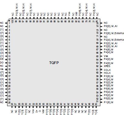 Specifications
| Symbol |
Description |
Min |
Typ |
Max |
Units |
Notes |
| TSTG |
Storage Temperature |
-55 |
25 |
+100 |
|
Higher storage temperatures will reduce data
retention time. Recommended storage temperature
is +25oC ± 25oC. Extended duration storage
temperatures above 65oC will degrade
reliability. |
| TA |
Ambient Temperature with Power Applied |
-40 |
|
+85 |
|
|
| Vdd |
Supply Voltage on Vdd Relative to Vss |
-0.5 |
|
+6.0 |
V |
|
| VIO |
DC Input Voltage |
Vss - 0.5 |
|
Vdd + 0.5 |
V |
|
| VIO2 |
DC Voltage Applied to Tri-state |
Vss - 0.5 |
|
Vdd + 0.5 |
V |
|
| IMIO |
Maximum Current into any Port Pin |
-25 |
|
+50 |
mA |
|
| IMAIO |
Maximum Current into any Port Pin Configured as Analog
Driver |
-50 |
|
+50 |
mA |
|
| ESD |
Electro Static Discharge Voltage |
2000 |
|
|
V |
Human Body Model ESD. |
| LU |
Latch-up Current |
|
|
200 |
mA |
|
DescriptionThe PSoC® family consists of many Mixed-Signal Array with On-Chip Controller devices,for example,CY8C24094.Like all PSoC family devices,CY8C24094 is designed to replace traditional MCUs, system ICs, and the numerous discrete components that surround them. The PSoC CY8C24x94 devices are unique members of the PSoC family because it includes a full-featured, full-speed (12 Mbps) USB port. Configurable analog, digital, and interconnect circuitry enable a high level of integration in a host of industrial, consumer, and communication applications.
This architecture of the CY8C24094 allows the user to create customized peripheral configurations that match the requirements of each individual application. Additionally, a fast CPU, Flash program memory, SRAM data memory, and configurable IO are included in a range of convenient pinouts and packages.
The PSoC architecture of the CY8C24094, as illustrated on the left, is comprised of four main areas: PSoC Core, Digital System, Analog System,and System Resources including a full-speed USB port. Configurable global busing allows all the device resources to be combined into a complete custom system. The PSoC CY8C24x94 devices can have up to seven IO ports that connect to the global digital and analog interconnects, providing access to 4 digital blocks and 6 analog blocks.

 CY8C24094, Data Sheet