Features: Double-buffered, single-buffered or flow-through digital data inputs
Easy interchange and pin-compatible with 12-bit DAC1230 series
Direct interface to all popular microprocessors
Linearity specified with zero and full scale adjust
only-NOT BEST STRAIGHT LINE FIT.
Works with ±10V reference-full 4-quadrant multiplication
Can be used in the voltage switching mode
Logic inputs which meet TTL voltage level specs (1.4V logic threshold)
Operates "STAND ALONE" (without P) if desired
Available in 20-pin small-outline or molded chip carrier packagePinout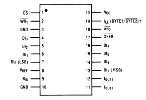 Specifications
| Resolution |
8 bits |
| Channels |
1 Channels |
| Interface Type |
Parallel |
| Settling Time |
1000 ns |
| Reference Source |
External |
| Max Supply Voltage |
5 Volt |
| Temperature Min |
-55 deg C |
| Temperature Max |
125 deg C |
| OtherSupply Voltage |
+5V to +15V |
| Tsettling Conditions |
1/2 LSB |
| Data Converter Type |
DAC |
| View Using Catalog |
Supply Voltage (VCC)............................................... 17 VDC
Voltage at Any Digital Input ...............................VCC to GND
Voltage at VREF Input .................................................±25V
Storage Temperature Range ....................−65°C to +150°C
Package Dissipation
at TA=25°C (Note 3)............................................... 500 mW
DC Voltage Applied to
IOUT1 or IOUT2 (Note 4)............................ −100 mV to VCC
ESD Susceptability (Note 4) .........................................800V
Lead Temperature (Soldering, 10 sec.)
Dual-In-Line Package (plastic) ...................................260°C
Dual-In-Line Package (ceramic) .................................300°C
Surface Mount Package
Vapor Phase (60 sec.) ...............................................215°C
Infrared (15 sec.) ......................................................220°CDescriptionThe DAC0830 is an advanced CMOS/Si-Cr 8-bit multiplying DAC designed to interface directly with the 8080, 8048, 8085, Z80®, and other popular microprocessors. A deposited silicon-chromium R-2R resistor ladder network divides the reference current and provides the circuit with excellent temperature tracking characteristics (0.05% of Full Scale Range maximum linearity error over temperature). The circuit uses CMOS current switches and control logic to achieve low power consumption and low output leakage current errors. Special circuitry provides TTL logic input voltage level compatibility.
Double buffering allows these DAC0830 to output a voltage corresponding to one digital word while holding the next digital word. This permits the simultaneous updating of any number of DACs.
The DAC0830 series are the 8-bit members of a family of microprocessor-compatible DACs (MICRO-DAC™).
Application Notes
| Title |
Size in Kbytes |
Date |
|
| AN-284: Application Note 284 Single-Supply Applications of CMOS MICRODACs |
121 Kbytes |
3-Oct-02 |
Download |
| AN-271: Application Note 271 Applying the New CMOS MICRO-DAC |
230 Kbytes |
4-Oct-04 |
Download |
AN-271 (Japanese): Application Note 271 Applying the New CMOS MICRO-DAC
640){this.height=this.height*640/this.width;this.width=640;}' border="0" alt=" Connection Diagram"> |
342 Kbytes |
|
|
If you have trouble printing or viewing PDF file(s), see Printing Problems.
|
The DAC0830 is an advanced CMOS/Si-Cr 8-bit multiplying DAC designed to interface directly with the 8080, 8048, 8085, Z80®, and other popular microprocessors. A deposited silicon-chromium R-2R resistor ladder network divides the reference current and provides the circuit with excellent temperature tracking characteristics (0.05% of Full Scale Range maximum linearity error over temperature). The circuit uses CMOS current switches and control logic to achieve low power consumption and low output leakage current errors. Special circuitry provides TTL logic input voltage level compatibility.
Double buffering allows these DACs to output a voltage corresponding to one digital word while holding the next digital word. This permits the simultaneous updating of any number of DACs.
The DAC0830 series are the 8-bit members of a family of microprocessor-compatible DACs (MICRO-DAC™).

 DAC0830 Data Sheet