Voltage Reference
:
Number of Converters
: 2
Interface Type
: Serial
Architecture
: Delta-Sigma
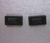
Packaging
: Tube
Input Type
: Voltage
Number of ADC Inputs
: 1
Supply Voltage - Max
: 5.25 V
Maximum Operating Temperature
: + 70 C
Supply Voltage - Min
: 4.75 V
Mounting Style
: Through Hole
Resolution
: 20 bit
Maximum Power Dissipation
: 275 mW
Conversion Rate
: 48 KSPs
SNR
: 110 dB
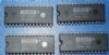
Package / Case
: DIP-28
Features: DUAL 20-BIT MONOLITHIC MODULATOR (PCM1760) AND MONOLITHIC DECIMATING DIGITAL FILTER (DF1760)
HIGH PERFORMANCE: THD+N: 92dB typ, 90dB max Dynamic Range: 108dB typ SNR: 108dB min, 110dB typ Channel Separation: 98dB typ, 94dB min
64X OVERSAMPLING
CO-PHASE CONVERSION
RUNS ON 256fs OR 384fs SYSTEM CLOCK
VERSATILE INTERFACE CAPABILITY: 16-, 20-Bit Output MSB First or LSB First Format
OPTIONAL FUNCTIONS: Offset Error Calibration Overflow Detection Power Down Mode (DF1760)
RUNS ON ±5V SUPPLIES (PCM1760) AND 5V SUPPLY (DF1760)
COMPACT 28-PIN PACKAGES: 28-Pin DIP and SOICPinout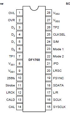 SpecificationsSupply Voltage .................................................................................... 7.0V
Voltage Mismatch ............................................................................... 0.1V
Digital Input ............................................................................... +VDD +0.5V
VSS 0.5V
Input Current ±20mA
Power Dissipation/P ....................................................................... 460mW
Power Dissipation/U ....................................................................... 440mW
Lead Temperature/P (soldering, 10s) .............................................. 260°C
Lead Temperature/U (soldering, 10s, reflow) ................................... 235°C
Operating Temperature .......................................................... 0°C to +70°c
Storage Temperature ...................................................... 50°C to +125°CDescriptionThe PCM1760 and DF1760 combine for a low-cost, high-performance dual 20-bit, 48kHz sampling analog- to-digital conversion system which is specifically designed for dynamic applications.
The PCM1760/DF1760 pair form a 4-bit, 4th order, 64X oversampling analog-to-digital converter.
The PCM1760 is a delta-sigma modulator that uses a 4-bit quantizer within the modulation loop to achieve very high dynamic range.
The DF1760 is a high-performance decimating digital filter. The DF1760 accepts 4-bit 64fs data from the PCM1760 and decimates to 20-bit 1fs data.
The FIR filter of the DF1760 has pass-band ripple of less than ±0.001dB and greater than 100dB of the reject band attenuation.
Parameters: | Technical/Catalog Information | DF1760P |
| Vendor | Texas Instruments |
| Category | Integrated Circuits (ICs) |
| Number of Bits | 20 |
| Package / Case | 28-DIP (600 mil) |
| Data Interface | Serial |
| Packaging | Tube |
| Sampling Rate (Per Second) | 192k |
| Operating Temperature | 0°C ~ 70°C |
| Voltage Supply Source | Analog and Digital, Dual ± |
| Number of Inputs and Type | 2 Single-Ended, Bipolar |
| Number of Converters | 2 |
| Power Dissipation (Max) | 275mW |
| Drawing Number | 296; 4040053; N; 24, 28, 40 |
| Lead Free Status | Contains Lead |
| RoHS Status | RoHS Non-Compliant |
| Other Names | DF1760P
DF1760P
|
 DF1760P Data Sheet