Features: Full function real time clockcalendar
--1224 hour mode timekeeping
--Day of week and day of years counters
--Four selectable oscillator frequencies
--Parallel Resonant Oscillator
Two 16-bit timers
--10 MHz external clock frequency
--Programmable multi-function output
--Flexible re-trigger facilities
Power fail features
--Internal power supply switch to external battery
--Power Supply Bus glitch protection
-- Automatic log of time into RAM at power failure
On-chip interrupt structure
--Periodic alarm timer and power fail interrupts
Up to 44 bytes of CMOS RAM
INTRMFOT1 pins programmable HighLow and push-pull or open drain
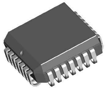
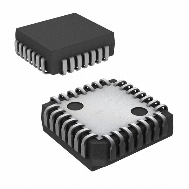
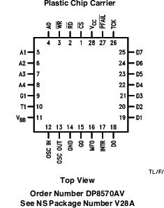
Pinout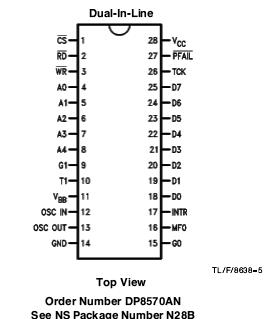
 SpecificationsSupplyVoltage(VCC)............................................................................- 0.5Vto+ 7.0V
DCInputVoltage(VIN).................................................................... -0.5VtoVCC +0.5V
DCOutputVoltage(VOUT).............................................................. -0.5VtoVCC+ 0.5V
StorageTemperatureRange .............................................................-65to +150
PowerDissipation(PD) ..................................................................................500mW
LeadTemperature(Soldering10sec) ................................................................260
| Application |
Timer Control Peripheral (TCP) |
| Temperature Min |
-40 deg C |
| Temperature Max |
85 deg C |
| PowerWise |
No |
| View Using Catalog |
DescriptionThe DP8570A is intended for use in microprocessor based systems where information is required for multi-tasking data logging or general time of daydate information. DP8570A is implemented in low voltage silicon gate microCMOS tech- nology to provide low standby power in battery back-up en- vironments .The circuit's architecture is such that it looks like a contiguous block of memory or IO ports The address space is organized as 2 software selectable pages of 32 bytes This includes the Control Registers the Clock Counters the Alarm Compare RAM the Timers and their data RAM and the Time Save RAM Any of the RAM locations that are not being used for their intended purpose may be used as general purpose CMOS RAM
Time and date are maintained from 1100 of a second to year and leap year in a BCD format 12 or 24 hour modes Day of week day of month and day of year counters are provided Time is controlled by an on-chip crystal oscillator requiring only the addition of the crystal and two capacitors The choice of crystal frequency is program selectable
Two independent multifunction 10 MHz 16-bit timers are provided These timers operate in four modes Each has its own prescaler and can select any of 8 possible clock inputs Thus by programming the input clocks and the timer counter values a very wide range of timing durations can be achieved The range is from about 400 ns (4915 MHz oscil-lator) to 65535 seconds (18 hrs 12 min)
Power failure logic and control functions of the DP8570A have been integrat- edonchipThislogicisusedbytheTCPtoissueapowerfail interrupt and lock out the mp interface The time power fails may be logged into RAM automatically when V
BB V
CC Additionally two supply pins are provided When V
BB V
CC internal circuitry will automatically switch from the main supply to the battery supply Status bits are provided to indicate initial application of battery power system power and lowbatterydetect

 DP8570A Data Sheet