DS10BR150TSD

PinoutDescriptionThe DS10BR150TSD is a single channel 1.0 Gbps LVDS buffer optimized for high-speed signal transmission over lossy FR-4 printed circuit board backplanes and balanced cables. The applications of it are: clock and data buffering, OC-12/STM-4, firewire 800. The features of DS10BR150T...

product image

DS10BR150TSD Picture
SeekIC No. : 004328406 Detail

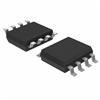
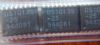
DS10BR150TSD: PinoutDescriptionThe DS10BR150TSD is a single channel 1.0 Gbps LVDS buffer optimized for high-speed signal transmission over lossy FR-4 printed circuit board backplanes and balanced cables. The appl...

floor Price/Ceiling Price

Part Number:
DS10BR150TSD
Supply Ability:
5000

Price Break

  • Qty
  • 1~5000
  • Unit Price
  • Negotiable
  • Processing time
  • 15 Days
Total Cost: $ 0.00

SeekIC Buyer Protection PLUS - newly updated for 2013!

  • Escrow Protection.
  • Guaranteed refunds.
  • Secure payments.
  • Learn more >>

Month Sales

268 Transactions

Rating

evaluate  (4.8 stars)

Upload time: 2024/4/30

Payment Methods

All payment methods are secure and covered by SeekIC Buyer Protection PLUS.

Notice: When you place an order, your payment is made to SeekIC and not to your seller. SeekIC only pays the seller after confirming you have received your order. We will also never share your payment details with your seller.
Product Details

Description


Pinout

  Connection Diagram


Description

The DS10BR150TSD is a single channel 1.0 Gbps LVDS buffer optimized for high-speed signal transmission over lossy FR-4 printed circuit board backplanes and balanced cables. The applications of it are: clock and data buffering, OC-12/STM-4, firewire 800.

The features of DS10BR150TSD can be summarized as:(1)DC - 1.0 Gbps low jitter, high noise immunity, low power operation; (2)On-chip 100 input and output termination minimizes; (3)insertion and return losses, reduces component count and minimizes board space; (4)7 kV ESD on LVDS I/O pins protects adjoining components; (5)Small 3 mm x 3 mm 8-LLP space saving package.

The absolute maximum ratings of DS10BR150TSD are:(1)Supply Voltage (VCC):-0.3V to +4V; (2)LVDS Input Voltage (IN+, IN-):-0.3V to +4V; (3)LVDS Differential Input Voltage  ((IN+) - (IN-)):0V to 1V; (4)LVDS Output Voltage  (OUT+, OUT-) -0.3V to (VCC +0.3V); (5)LVDS Differential Output Voltage  ((OUT+) - (OUT-)):0V to 1V; (6)LVDS Output Short Circuit Current Duration:5 ms; (7)Junction Temperature:+150°C; (8)Storage Temperature Range:-65°C to +150°C; (9)Lead Temperature Range Soldering (4 sec.):+260°C; (10)Maximum Package Power Dissipation at 25°C:SDA Package..2.08W, Derate SDA Package..16.7 mW/°C above +25°C; (11)Package Thermal Resistance:JA..+60.0°C/W,JC..+12.3°C/W; (12)HBM 7 kV; (13)MM 250V; (14)CDM 1250V.

If you want to know more information such as the electrical characteristics about the DS10BR150TSD, please download the datasheet in www.seekic.com or www.chinaicmart.com .


Customers Who Bought This Item Also Bought

Margin,quality,low-cost products with low minimum orders. Secure your online payments with SeekIC Buyer Protection.
Programmers, Development Systems
Optoelectronics
Batteries, Chargers, Holders
Line Protection, Backups
Integrated Circuits (ICs)
Cables, Wires - Management
View more