Features: ·Single +3.3 V Supply
·B/LVDS receiver inputs accept LVPECL signals
·TRI-STATE outputs
·Loss of Signal (LOS ) pin detects a non-driven bus
·Receiver input threshold < ±100 mV
·Fast propagation delay of 1.4 ns (typ)
·Low jitter 400 Mbps fully differential data path
·Compatible with BLVDS 10-bit SerDes (40MHz)
·Compatible with ANSI/TIA/EIA-644-A LVDS standard
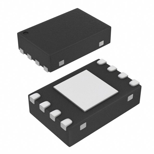
·Available in SOIC and space saving LLP package
·Industrial Temperature RangePinout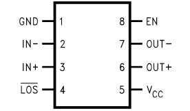 SpecificationsSupply Voltage (VCC) −0.3V to +4V
LVCMOS/LVTTL Input Voltage (EN) −0.3V to (VCC + 0.3V)
LVCMOS/LVTTL Output Voltage (LOS ) −0.3V to (VCC + 0.3V)
B/LVDS Receiver Input Voltage (IN+, IN−) −0.3V to +4V
BLVDS Driver Output Voltage (OUT+, OUT−) −0.3V to +4V
BLVDS Output Short Circuit Current Continuous
Junction Temperature +150°C
Storage Temperature Range −65°C to +150°C
Lead Temperature Range
Soldering (4 sec.) +260°C
M Package 726 mW
Derate M Package 5.8 mW/°C above +25°C
LDA Package 2.44 W
Derate LDA Package 19.49 mW/°C above +25°C
ESD Ratings
(HBM, 1.5kΩ, 100pF) 2.5kV
(EIAJ, 0Ω, 200pF) 250VDescriptionThe DS92001 B/LVDS-BLVDS Buffer takes a BLVDS input signal and provides an BLVDS output signal. In many large systems, signals are distributed across backplanes, and one of the limiting factors for system speed is the 'stub length' or the distance between the transmission line and the unterminated receivers on individual cards. Although it is generally recognized that this distance should be as short as possible to maximize system performance, real-world packaging concerns often make it difficult to make the stubs as short as the designer would like.
The DS92001 has edge transitions optimized for multidrop backplanes where the switching frequency is in the 200 MHz range or less. The output edge rate is critical in some systems where long stubs may be present, and utilizing a slow transition allows for longer stub lengths.
The DS92001, available in the LLP (Leadless Leadframe Package) package, will allow the receiver inputs to be placed very close to the main transmission line, thus improving system performance.
A wide input dynamic range allows the DS92001 to receive differential signals from LVPECL as well as LVDS sources. This will allow the device to also fill the role of an LVPECLBLVDS translator.
The LOS pin detects a non-driven B/LVDS bus state at the input and provides an active LOW output. The LOS pin can be tied to the device's output enable pin (EN) to generate a TRI-STATE output state when the input is un-driven. The LOS pin can also be used locally to inform the system of the bus state.

 DS92001 Data Sheet