Features: ·Clock recovery from PLL lock to random data patterns.
·Guaranteed transition every data transfer cycle
·Chipset (Tx + Rx) power consumption < 500 mW (typ) @ 66 MHz
·Single differential pair eliminates multi-channel skew
·Flow-through pinout for easy PCB layout
·660 Mbps serial Bus LVDS data rate (at 66 MHz clock)
·10-bit parallel interface for 1 byte data plus 2 control bits
·Synchronization mode and LOCK indicator
·Programmable edge trigger on clock
·High impedance on receiver inputs when power is off
·Bus LVDS serial output rated for 27Ω load
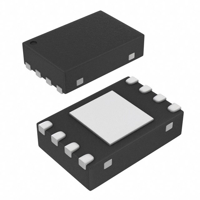
·Small 28-lead SSOP packagePinout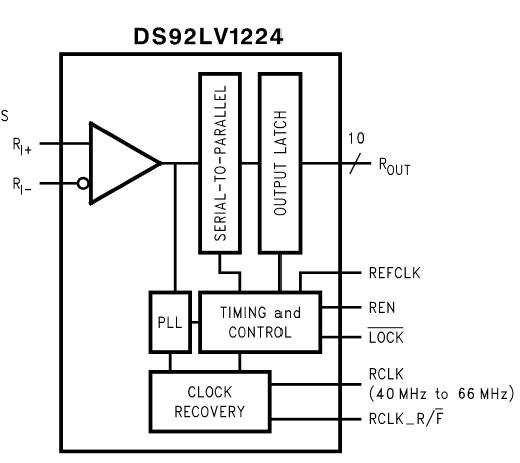 SpecificationsSupply Voltage (VCC) −0.3V to +4V
LVCMOS/LVTTL Input Voltag −0.3V to (VCC +0.3V)
LVCMOS/LVTTL Output Voltage−0.3V to (VCC +0.3V)
Bus LVDS Receiver Input Voltage −0.3V to +3.9V
Bus LVDS Driver Output Voltage −0.3V to +3.9V
Bus LVDS Output Short Circuit Duration10mS
Junction Temperature +150°C
Storage Temperature−65°C to +150°C
Lead Temperature (Soldering, 4 seconds)+260°C
Maximum Package Power Dissipation Capacity @25°C
Package: 28L SSOP 1.27 W
Package Derating:28L SSOP 10.3 mW/°C
above +25°C
ja 97°C/W
jc 27°C/W
ESD Rating for DS92LV1023
HBM (1.5kOhm, 100pF) >1kV
MM > 250V
ESD Rating for DS92LV1224
HBM (1.5kOhm, 100pF) >2kV
MM > 250V
| Function |
Deserializer |
| Total Throughput |
660 Mbps |
| Payload/Channel |
660 Mbps |
| Clock Min |
30 MHz |
| Clock Max |
66 MHz |
| Input Compatibility |
LVDS/BLVDS |
| Output Compatibility |
LVTTL |
| Start/Stop Bit |
Yes |
| Power Consumption_ |
192 mW |
| SupplyVoltage |
3.3 Volt |
| Eval Kit |
BLVDS03 |
| ESD |
2 kV |
| Temperature Min |
-40 deg C |
| Temperature Max |
85 deg C |
| Compression Ratio |
10:1 |
| Number Receivers |
1 |
| Communications |
Yes |
| Sensing & Imaging |
Yes |
| Parallel Bus Width |
10 bits |
| View Using Catalog |
DescriptionThe DS92LV1023 transforms a 10-bit wide parallel LVCMOS/LVTTL data bus into a single high speed Bus LVDS serial data stream with embedded clock.
The DS92LV1224 receives the Bus LVDS serial data stream and transforms it back into a 10-bit wide parallel data bus and recovers parallel clock. The DS92LV1023 transmits data over backplanes or cable. The single differential pair data path makes PCB design easier. In addition, the reduced cable, PCB trace count, and connector size tremendously reduce cost. Since one output transmits clock and data bits serially, it eliminates clock-to-data and data-to-data skew.
The DS92LV1224 powerdown pin saves power by reducing supply current when not using either device. Upon power up of the Serializer, you can choose to activate synchronization mode or allow the Deserializer to use the synchronization-to-random-data feature. By using the synchronization mode, the Deserializer will establish lock to a signal within specified lock times. In addition, the embedded clock guarantees a transition on the bus every 12-bit cycle.
This DS92LV1224 eliminates transmission errors due to charged cable conditions. Furthermore, you may put the DS92LV1023 output pins into TRI-STATE ® to achieve a high impedance state. The PLL can lock to frequencies between 40 MHz and 66 MHz.

 DS92LV1224 Data Sheet