DS99R102

Features: ` 3 MHz40 MHz clock embedded and DC-Balancing 24:1 and 1:24 data transmissions` User selectable clock edge for parallel data on both Transmitter and Receiver` Internal DC Balancing encode/decode Supports ACcoupling interface with no external coding required` Individual power-down contro...

product image

DS99R102 Picture
SeekIC No. : 004329477 Detail

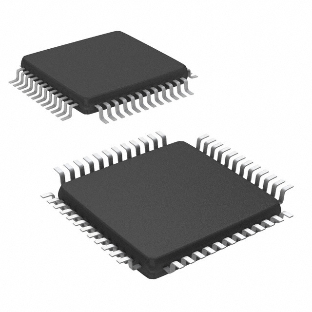
DS99R102: Features: ` 3 MHz40 MHz clock embedded and DC-Balancing 24:1 and 1:24 data transmissions` User selectable clock edge for parallel data on both Transmitter and Receiver` Internal DC Balancing encode/...

floor Price/Ceiling Price

Part Number:
DS99R102
Supply Ability:
5000

Price Break

  • Qty
  • 1~5000
  • Unit Price
  • Negotiable
  • Processing time
  • 15 Days
Total Cost: $ 0.00

SeekIC Buyer Protection PLUS - newly updated for 2013!

  • Escrow Protection.
  • Guaranteed refunds.
  • Secure payments.
  • Learn more >>

Month Sales

268 Transactions

Rating

evaluate  (4.8 stars)

Upload time: 2024/5/5

Payment Methods

All payment methods are secure and covered by SeekIC Buyer Protection PLUS.

Notice: When you place an order, your payment is made to SeekIC and not to your seller. SeekIC only pays the seller after confirming you have received your order. We will also never share your payment details with your seller.
Product Details

Description


Features:

` 3 MHz40 MHz clock embedded and DC-Balancing 24:1
  and 1:24 data transmissions
` User selectable clock edge for parallel data on both
  Transmitter and Receiver
` Internal DC Balancing encode/decode Supports ACcoupling
  interface with no external coding required
` Individual power-down controls for both Transmitter and Receiver
` Embedded clock CDR (clock and data recovery) on
  Receiver and no external source of reference clock needed
` All codes RDL (random data lock) to support livepluggable applications
` LOCK output flag to ensure data integrity at Receiver side
` Balanced TSETUP/THOLD between RCLK and RDATA on
  Receiver side
` PTO (progressive turn-on) LVCMOS outputs to reduce
  EMI and minimize SSO effects
` All LVCMOS inputs and control pins have internal pulldown
` On-chip filters for PLLs on Transmitter and Receiver
` 48-pin TQFP package
` Pure CMOS .35 m process
` Power supply range 3.3V ± 10%
` Temperature range 0°C to +70°C
` 8 kV HBM ESD tolerance


Specifications

If Military/Aerospace specified devices are required,
please contact the National Semiconductor Sales Office/
Distributors for availability and specifications.
Supply Voltage (VDD) ...................................................−0.3V to +4V
LVCMOS/LVTTL Input Voltage ..........................−0.3V to (VDD +0.3V)
LVCMOS/LVTTL Output Voltage ........................−0.3V to (VDD +0.3V)
LVDS Receiver Input Voltage .......................................−0.3V to 3.9V
LVDS Driver Output Voltage .........................................−0.3V to 3.9V
LVDS Output Short Circuit Duration .........................................10 ms
Junction Temperature ...........................................................+150°C
Storage Temperature ............................................−65°C to +150°C
Lead Temperature
(Soldering, 4 seconds).......................................................... +260°C
Maximum Package Power Dissipation Capacity Package
De-rating:
48L TQFP 1/JA °C/W above ...................................................+25°C
DS99R101
JA ........................................................45.8 (4L*); 75.4 (2L*) °C/W
JC.................................................................................... 21.0°C/W
DS99R102
JA .........................................................45.4 (4L*); 75.0 (2L*)°C/W
JC.................................................................................... 21.1°C/W
*JEDEC
ESD Rating (HBM) ..................................................................±8 kV


Description

The DS99R101/DS99R102 Chipset translates a 24-bit parallel bus into a fully transparent data/control LVDS serial stream with embedded clock information. This single serial stream simplifies transferring a 24-bit bus over PCB traces and cable by eliminating the skew problems between parallel data and clock paths. It saves system cost by narrowing data paths that in turn reduce PCB layers, cable width, and connector size and pins.

The DS99R101/DS99R102 incorporates LVDS signaling on the high-speed I/O. LVDS provides a low power and low noise environment for reliably transferring data over a serial transmission path. By optimizing the serializer output edge rate for the operating frequency range EMI is further reduced.

DS99R101/DS99R102 Internal DC balanced encoding/decoding is used to support AC-Coupled interconnects.


Customers Who Bought This Item Also Bought

Margin,quality,low-cost products with low minimum orders. Secure your online payments with SeekIC Buyer Protection.
Computers, Office - Components, Accessories
Discrete Semiconductor Products
Soldering, Desoldering, Rework Products
Power Supplies - Board Mount
Transformers
Circuit Protection
View more