EN25F05

DescriptionThe EN25F05 is a 512K-bit (64K-byte) Serial Flash memory, with advanced write protection mechanisms, accessed by a high speed SPI-compatible bus. The memory can be programmed 1 to 256 bytes at a time, using the Page Program instruction.The EN25F05 is designed to allow either single Sect...

product image

EN25F05 Picture
SeekIC No. : 004336558 Detail

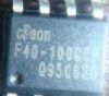
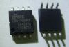
EN25F05: DescriptionThe EN25F05 is a 512K-bit (64K-byte) Serial Flash memory, with advanced write protection mechanisms, accessed by a high speed SPI-compatible bus. The memory can be programmed 1 to 256 byt...

floor Price/Ceiling Price

Part Number:
EN25F05
Supply Ability:
5000

Price Break

  • Qty
  • 1~5000
  • Unit Price
  • Negotiable
  • Processing time
  • 15 Days
Total Cost: $ 0.00

SeekIC Buyer Protection PLUS - newly updated for 2013!

  • Escrow Protection.
  • Guaranteed refunds.
  • Secure payments.
  • Learn more >>

Month Sales

268 Transactions

Rating

evaluate  (4.8 stars)

Upload time: 2024/4/28

Payment Methods

All payment methods are secure and covered by SeekIC Buyer Protection PLUS.

Notice: When you place an order, your payment is made to SeekIC and not to your seller. SeekIC only pays the seller after confirming you have received your order. We will also never share your payment details with your seller.
Product Details

Description


Description

The EN25F05 is a 512K-bit (64K-byte) Serial Flash memory, with advanced write protection mechanisms, accessed by a high speed SPI-compatible bus. The memory can be programmed 1 to 256 bytes at a time, using the Page Program instruction.The EN25F05 is designed to allow either single Sector at a time or full chip erase operation. The EN25F05 can be configured to protect part of the memory as the software protected mode. The device can sustain a minimum of 100K program/erase cycles on each sector.

Features of the EN25F05 are:(1)lockable 256 byte OTP security sector; (2)minimum 100K endurance cycle; (3)industrial temperature range; (4)write protect all or portion of memory via software; (5)enable/disable protection with WP# pin.The SPI Serial Data Input (DI) pin provides a means for instructions, addresses and data to be serially written to (shifted into) the device. Data is latched on the rising edge of the Serial Clock (CLK) input pin.

The absolute maximum ratings of the EN25F05 can be summarized as:(1)storage temperature:-65 to 125;(2)plastic packages:-65 to 125;(3)output short circuit current:200mA;(4)input and output voltage:-0.5 to 4.0 V;(5)Vcc:-0.5 to 4.0V.Stresses above the values so mentioned above may cause permanent damage to the device. These values are for a stress rating only and do not imply that the device should be operated at conditions up to or above these values. Exposure of the device to the maximum rating values for extended periods of time may adversely affect the device reliability.The first byte addressed can be at any location.The address is automatically incremented to the next higher address after each byte of data is shifted out. The whole memory can, therefore, be read with a single Read Data Bytes at Higher Speed (FAST_READ) instruction. When the highest address is reached, the address counter rolls over to 000000h, allowing the read sequence to be continued indefinitely.


Customers Who Bought This Item Also Bought

Margin,quality,low-cost products with low minimum orders. Secure your online payments with SeekIC Buyer Protection.
Potentiometers, Variable Resistors
Industrial Controls, Meters
Static Control, ESD, Clean Room Products
Inductors, Coils, Chokes
Circuit Protection
Test Equipment
View more