Features: ` 5.0V ± 10%, single power supply operation
- Minimizes system level power requirements
` Manufactured on 0.32 m process technology
` High performance
- Access times as fast as 45 ns
` Low power consumption
- 25 mA typical active read current
- 30 mA typical program/erase current
- 1 A typical standby current (standard access time to active mode)
` Flexible Sector Architecture:
- One 16 Kbyte, two 8 Kbyte, one 32 Kbyte, and fifteen 64 Kbyte sectors (byte mode)
- One 8 Kword, two 4 Kword, one 16 Kword and fifteen 32 Kword sectors (word mode)
- Supports full chip erase
- Individual sector erase supported
- Sector protection: Hardware locking of sectors to prevent program or erase operations within individual sectors Additionally, temporary Sector Group Unprotect allows code changes in previously locked sectors.
` High performance program/erase speed
- Byte program time: 10s typical
- Sector erase time: 500ms typical
- Chip erase time: 3.5s typical
` Low Standby Current
- 1A CMOS standby current-typical
- 1mA TTL standby current
` Low Power Active Current
- 30mA active read current
- 30mA program/erase current
` JEDEC Standard program and erase commands
` JEDEC standard DATA polling and toggle bits feature
` Single Sector and Chip Erase
` Sector Unprotect Mode
` Embedded Erase and Program Algorithms
` Erase Suspend / Resume modes: Read and program another Sector during Erase Suspend Mode
` 0.32 m double-metal double-poly triple-well CMOS Flash Technology
` Low Vcc write inhibit < 3.2V
` >100K program/erase endurance cycle
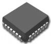
` 48-pin TSOP (Type 1)
` Commercial Temperature Range
Pinout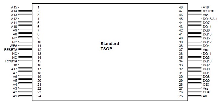 Specifications
|
Parameter |
Value |
Unit |
| Storage Temperature |
-65 to +125 |
|
| Plastic Packages |
-65 to +125 |
|
Ambient Temperature
With Power Applied |
-55 to +125 |
|
| Output Short Circuit Current1 |
200 |
mA |
Voltage with
Respect to Ground |
A9, OE#, Reset# 2 |
-0.5 to +11.5 |
V |
| All other pins 3 |
-0.5 to Vcc+0.5 |
V |
| Vcc |
-0.5 to +7.0 |
V |
Notes:
1. No more than one output shorted at a time. Duration of the short circuit should not be greater than one second.
2. Minimum DC input voltage on A9, OE#, RESET# pins is 0.5V. During voltage transitions, A9, OE#, RESET# pins may
undershoot Vss to 1.0V for periods of up to 50ns and to 2.0V for periods of up to 20ns. See figure below. Maximum DC input voltage on A9, OE#, and RESET# is 11.5V which may overshoot to 12.5V for periods up to 20ns.
3. Minimum DC voltage on input or I/O pins is 0.5 V. During voltage transitions, inputs may undershoot Vss to 1.0V for periods of up to 50ns and to 2.0 V for periods of up to 20ns. See figure below. Maximum DC voltage on output and I/O pins is Vcc +0.5 V. During voltage transitions, outputs may overshoot to Vcc + 2.0 V for periods up to 20ns. See figure below.
4. Stresses above the values so mentioned above may cause permanent damage to the device. These values are for a stress rating only and do not imply that the device should be operated at conditions up to or above these values.
Exposure of the device to the maximum rating values for extended periods of time may adversely affect the device reliability.
DescriptionThe EN29F800 is a 8-Megabit, electrically erasable, read/write non-volatile flash memory, organized as 1,048,576 bytes or 524,288 words. Any byte can be programmed typically in 10s. The EN29F800 features 5.0V voltage read and write operation, with access times as fast as 45ns to eliminate the need for WAIT states in high-performance microprocessor systems.
The EN29F800 has separate Output Enable (OE), Chip Enable ( CE ), and Write Enable ( WE ) controls, which eliminate bus contention issues. This device is designed to allow either single (or multiple) Sector or full chip erase operation, where each Sector can be individually protected against program/erase operations or temporarily unprotected to erase or program. The device can sustain a minimum of 100K program/erase cycles on each Sector.

 EN29F800 Data Sheet