Features: • 8-bit BTL transceivers
• Separate I/O on TTL A-port
• Inverting
• Drives heavily loaded backplanes with equivalent load impedances down to 10.
• High drive 100mA BTL open collector drivers on B-port
• Allows incident wave switching in heavily loaded backplane buses
• Reduced BTL voltage swing produces less noise and reduces power consumption
• Built-in precision band-gap reference provides accurate receiver thresholds and improved noise immunity
• Compatible with IEEE Futurebus+ or proprietary BTL backplanes
• Controlled output ramp and multiple GND pins minimize ground bounce
• Each BTL driver has a dedicated Bus GND for a signal return
• Glitch-free power up/power down operation
• Low ICC current
• Tight output skew
• Supports live insertion
• Pins for the optional JTAG boundary scan function are provided
• High density packaging in plastic Quad Flat PackPinout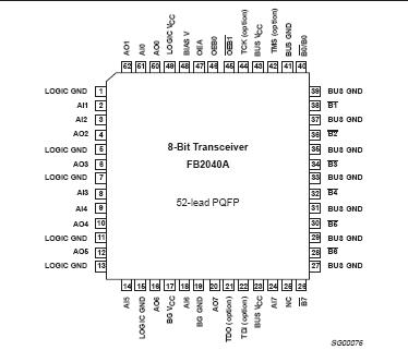 Specifications
| SYMBOL |
PARAMETER |
RATING |
UNIT |
| VCC |
Supply voltage |
-0.5 to +7.0 |
V |
| VIN |
Input voltage |
AI0 AI7,OEB0, OEB1, OEA |
-1.2 to +7.0 |
V |
| B0 B7 |
-1.2 to +5.5 |
| IIN |
Input current |
-18 to +5.0 |
mA |
| VOUT |
Voltage applied to output in High output state |
-0.5 to +VCC |
V |
| LOUT |
Current applied to output in Low
output state |
A0 A7 |
48 |
mA |
| B0 B7 |
200 |
| Tamb |
Operating free-air temperature range |
-40 to ++85 |
°C |
| TSTG |
Storage temperature |
-65 to +150 |
°C |
DescriptionThe FB2040A is an 8-bit bidirectional BTL transceiver and is intended to provide the electrical interface to a high performance wired-OR bus. The FB2040A is an inverting transceiver.
The FB2040A B-port drivers are Low-capacitance open collectors with controlled ramp and are designed to sink 100mA. Precision band gap references on the B-port insure very good noise margins by limiting the switching threshold to a narrow region centered at 1.55V.
The FB2040A B-port interfaces to "Backplane Transceiver Logic" (See the IEEE 1194.1 BTL standard). BTL features low power consumption by reducing voltage swing (1Vp-p, between 1V and 2V) and reduced capacitive loading by placing an internal series diode on the drivers. BTL also provides incident wave switching, a necessity for high performance backplanes.
The FB2040A A-port operates at TTL levels with separate I/O. The 3-state A-port drivers are enabled when OEA goes High after an extra 6ns delay which is built in to provide a break-before-make function. When OEA goes Low, A-port drivers become High impedance without any extra delay. During power on/off cycles, the A-port drivers are held in a High impedance state when VCC is below 2.5V.
The FB2040A B-port has two output enables, OEB0 and OEB1. When OEB0 is High and OEB1 is Low the output is enabled. When OEB0 is Lowor if OEB1 is High, the B-port is inactive and is at the level of the backplane signal.
To support live insertion, FB2040A OEB0 is held Low during power on/off cycles to insure glitch free B port drivers. Proper bias for B port drivers during live insertion is provided by the BIAS V pin when at a 5V level while VCC is Low. If live insertion is not a requirement, the BIAS V pin should be tied to a VCC pin.
The FB2040A LOGIC GND and BUS GND pins are isolated in the package to minimize noise coupling between the BTL and TTL sides. These pins should be tied to a common ground external to the package.
Each FB2040A BTL driver has an associated BUS GND pin that acts as a signal return path and these BUS GND pins are internally isolated from each other. In the event of a ground return fault, a "hard" signal failure occurs instead of a pattern dependent error that may be very infrequent and impossible to trouble-shoot.
The FB2040A LOGIC VCC and BUS VCC pins are also isolated internally to minimize noise and may be externally decoupled separately or simply tied together.
FB2040A JTAG boundary scan pins are provided with signals TMS, TCK, TDI and TDO. TMS and TCK are no-connects (no bond wires) and TDI and TDO are shorted together internally. Boundary scan functionality is not implemented at this time.

 FB2040A Data Sheet