FBL2041I

Features: • 7-bit BTL transceiver• Separate I/O on TTL A-port• Inverting• Three separate pairs of driver enables in a 1 bit, 3 bit, 3 bit arrangement• Drives heavily loaded backplanes with equivalent load impedances down to 10W.• High drive 100mA BTL open collec...

product image

FBL2041I Picture
SeekIC No. : 004340720 Detail

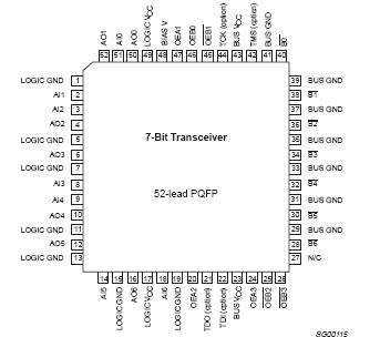
FBL2041I: Features: • 7-bit BTL transceiver• Separate I/O on TTL A-port• Inverting• Three separate pairs of driver enables in a 1 bit, 3 bit, 3 bit arrangement• Drives heavily lo...

floor Price/Ceiling Price

Part Number:
FBL2041I
Supply Ability:
5000

Price Break

  • Qty
  • 1~5000
  • Unit Price
  • Negotiable
  • Processing time
  • 15 Days
Total Cost: $ 0.00

SeekIC Buyer Protection PLUS - newly updated for 2013!

  • Escrow Protection.
  • Guaranteed refunds.
  • Secure payments.
  • Learn more >>

Month Sales

268 Transactions

Rating

evaluate  (4.8 stars)

Upload time: 2024/4/22

Payment Methods

All payment methods are secure and covered by SeekIC Buyer Protection PLUS.

Notice: When you place an order, your payment is made to SeekIC and not to your seller. SeekIC only pays the seller after confirming you have received your order. We will also never share your payment details with your seller.
Product Details

Description


Features:

• 7-bit BTL transceiver
• Separate I/O on TTL A-port
• Inverting
• Three separate pairs of driver enables in a 1 bit, 3 bit, 3 bit arrangement
• Drives heavily loaded backplanes with equivalent load impedances down to 10W.
• High drive 100mA BTL open collector drivers on B-port
• Allows incident wave switching in heavily loaded backplane buses
• Reduced BTL voltage swing produces less noise and reduces power consumption
• Built-in precision band-gap reference provides accurate receiver thresholds and improved noise immunity
• Compatible with IEEE Futurebus+ or proprietary BTL backplanes
• Controlled output ramp and multiple GND pins minimize ground bounce
• Each BTL driver has a dedicated Bus GND for a signal return
• Glitch-free power up/power down operation
• Low ICC current
• Tight output skew
• Supports live insertion
• Pins for the optional JTAG boundary scan function are provided
• High density packaging in plastic Quad Flatpack
• 5V compatible I/O on A-port
• Industrial temperature range option available as FBL2041I


Pinout

  Connection Diagram


Specifications

SYMBOL PARAMETER RATING UNIT
VCC Supply voltage -0.5 to +4.6 V
VIN Input voltage AI0 AI6, OEB0, OEBn, OEAn -0.5 to +7.0 V
B0 B6 -0.5 to +3.5
IIN Input current VIN < 0 -50
VOUT Voltage applied to output in High output state -0.5 to +7.0 V
LOUT Current applied to output in Lowoutput state AO0 AO6 64, 64 mA
B0 B6 200
TSTG Storage temperature -65 to +150 °C


Description

The FBL2041/FBL2041I is a 7-bit bidirectional BTL transceiver and is intended to provide the electrical interface to a high performance wired-OR bus. The FBL2041 is an inverting transceiver.

The FBL2041/FBL2041I B-port drivers are Low-capacitance open collectors with controlled ramp and are designed to sink 100mA. Precision band gap references on the B-port insure very good noise margins by limiting the switching threshold to a narrow region centered at 1.55V.

The FBL2041/FBL2041I is pin and function compatible with FB2041 but operates at a 3.3V supply voltage, greatly reducing power consumption.

The FBL2041/FBL2041I B-port interfaces to "Backplane Transceiver Logic" (See the IEEE 1194.1 BTL standard). BTL features low power consumption by reducing voltage swing (1Vp-p, between 1V and 2V) and reduced capacitive loading by placing an internal series diode on the drivers. BTL also provides incident wave switching, a necessity for high performance backplanes.

There are three separate pairs of driver enables in a 1 bit, 3 bit, 3 bit arrangement. The FBL2041/FBL2041I TTL/BTL output drivers for bit 0 are enabled with OEA1/OEB1, output drivers for bits 123 are enabled with OEA2/OEB2 and output drivers for bits 456 are enabled with OEA3/OEB3.

The FBL2041/FBL2041I A-port operates at TTL levels with separate I/O. The 3-state A-port drivers are enabled when OEAn goes High after an extra 6ns delay which is built in to provide a break-before-make function. When OEAn goes Low, A-port drivers become High impedance without any extra delay. During power on/off cycles, the A-port drivers are held in a High impedance state when VCC is below 1.3V.

The FBL2041/FBL2041I B-port has an output enable, OEB0, which affects all seven drivers. When OEB0 is High and OEBn is Low the output driver will be enabled. When OEB0 is Low or if OEBn is High, the B-port drivers will be inactive and at the level of the backplane signal.

To support live insertion, FBL2041/FBL2041I OEB0 is held Low during power on/off cycles to insure glitch free B port drivers. Proper bias for B port drivers during live insertion is provided by the BIAS V pin when at a 3.3V level while VCC is Low. If live insertion is not a requirement, the BIAS V pin should be tied to a VCC pin.

The LOGIC GND and BUS GND pins are isolated in the package to minimize noise coupling between the BTL and TTL sides. These pins should be tied to a common ground external to the package.

Each BTL driver has an associated BUS GND pin that acts as a signal return path and these BUS GND pins are internally isolated from each other. In the event of a ground return fault, a "hard" signal failure occurs instead of a pattern dependent error that may be very infrequent and impossible to trouble-shoot.

JTAG boundary scan functionality is provided as an option with signals TMS, TCK, TDI and TDO. When this option is not present, TMS and TCK are no-connects (no bond wires) and TDI and TDO are shorted together internally.


Customers Who Bought This Item Also Bought

Margin,quality,low-cost products with low minimum orders. Secure your online payments with SeekIC Buyer Protection.
Connectors, Interconnects
Soldering, Desoldering, Rework Products
Test Equipment
Boxes, Enclosures, Racks
Audio Products
Memory Cards, Modules
View more