FDC6333C

MOSFET 30V/-30V N/P

product image

FDC6333C Picture
SeekIC No. : 00149220 Detail

FDC6333C: MOSFET 30V/-30V N/P

floor Price/Ceiling Price

US $ .15~.29 / Piece | Get Latest Price
Part Number:
FDC6333C
Mfg:
Fairchild Semiconductor
Supply Ability:
5000

Price Break

  • Qty
  • 0~1
  • 1~25
  • 25~100
  • 100~250
  • Unit Price
  • $.29
  • $.23
  • $.17
  • $.15
  • Processing time
  • 15 Days
  • 15 Days
  • 15 Days
  • 15 Days
View more price & deliveries
Total Cost: $ 0.00

SeekIC Buyer Protection PLUS - newly updated for 2013!

  • Escrow Protection.
  • Guaranteed refunds.
  • Secure payments.
  • Learn more >>

Month Sales

268 Transactions

Rating

evaluate  (4.8 stars)

Upload time: 2024/4/26

Payment Methods

All payment methods are secure and covered by SeekIC Buyer Protection PLUS.

Notice: When you place an order, your payment is made to SeekIC and not to your seller. SeekIC only pays the seller after confirming you have received your order. We will also never share your payment details with your seller.
Product Details

Quick Details

Transistor Polarity : N and P-Channel Drain-Source Breakdown Voltage : - 30 V
Gate-Source Breakdown Voltage : +/- 16 V, +/- 25 V Continuous Drain Current : + 2.5 A, - 2 A
Resistance Drain-Source RDS (on) : 0.095 Ohms Configuration : Dual
Maximum Operating Temperature : + 150 C Mounting Style : SMD/SMT
Package / Case : SSOT-6 Packaging : Reel    

Description

Mounting Style : SMD/SMT
Packaging : Reel
Maximum Operating Temperature : + 150 C
Configuration : Dual
Transistor Polarity : N and P-Channel
Drain-Source Breakdown Voltage : - 30 V
Resistance Drain-Source RDS (on) : 0.095 Ohms
Package / Case : SSOT-6
Gate-Source Breakdown Voltage : +/- 16 V, +/- 25 V
Continuous Drain Current : + 2.5 A, - 2 A


Features:

` Q1 2.5 A, 30V. RDS(ON) = 95 mW @ VGS = 10 V RDS(ON) = 150 mW @ VGS = 4.5 V
` Q2 2.0 A, 30V. RDS(ON) = 150 mW @ VGS = 10 V RDS(ON) = 220 mW @ VGS = 4.5 V
` Low gate charge
` High performance trench technology for extremely low RDS(ON).
` SuperSOT 6 package: small footprint (72% smaller than SO-8); low profile (1mm thick).


Application

· DC/DC converter
· Load switch
· LCD display inverter


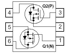
Pinout

  Connection Diagram


Specifications

Symbol
Parameter
Q1
Q2
Units
VDSS
VGSS
Drain-Source Voltage
Gate-Source Voltage
30
±16
2.5
8
30
±25
2.0
8
V
V
A
ID
Drain Current Continuous
Pulsed
(Note 1a)
PD
Power Dissipation for Single Operation
(Note 1a)
(Note 1b)
(Note 1c)
0.96
0.9
0.7
W
TJ, TSTG
Operating and Storage Junction Temperature Range
55 to +150
°C


Description

These FDC6333C N & P-Channel MOSFETs are produced using Fairchild Semiconductor's advanced PowerTrench process that has been especially tailored to minimize on-state resistance and yet maintain superior switching performance. These devices FDC6333C have been designed to offer exceptional power dissipation in a very small footprint for applications where the bigger more expensive SO-8 and TSSOP-8 packages are impractical.


Parameters:

Technical/Catalog InformationFDC6333C
VendorFairchild Semiconductor (VA)
CategoryDiscrete Semiconductor Products
Mounting TypeSurface Mount
FET PolarityN and P-Channel
Drain to Source Voltage (Vdss)30V
Current - Continuous Drain (Id) @ 25° C2.5A, 2A
Rds On (Max) @ Id, Vgs95 mOhm @ 2.5A, 10V
Input Capacitance (Ciss) @ Vds 282pF @ 15V
Power - Max700mW
PackagingCut Tape (CT)
Gate Charge (Qg) @ Vgs6.6nC @ 10V
Package / CaseSuperSOT-6
FET FeatureLogic Level Gate
Drawing Number*
Lead Free StatusLead Free
RoHS StatusRoHS Compliant
Other Names FDC6333C
FDC6333C
FDC6333CCT ND
FDC6333CCTND
FDC6333CCT


Customers Who Bought This Item Also Bought

Margin,quality,low-cost products with low minimum orders. Secure your online payments with SeekIC Buyer Protection.
Audio Products
Industrial Controls, Meters
Transformers
Static Control, ESD, Clean Room Products
Resistors
Undefined Category
View more