Transistor Polarity
: N-Channel
Gate-Source Breakdown Voltage
: +/- 20 V
Mounting Style
: SMD/SMT
Packaging
: Reel
Drain-Source Breakdown Voltage
: 30 V
Maximum Operating Temperature
: + 150 C
Configuration
: Dual Dual Drain
Package / Case
: SOIC-8 Narrow
Resistance Drain-Source RDS (on)
: 0.016 Ohms
Continuous Drain Current
: 6.3 A, 8.6 A
Features: • Q2: Optimized to minimize conduction losses Includes SyncFET Schottky body diode
8.6A, 30V = 0.016Ω @ VGS = 10V R DS(on)
= 0.021Ω @ VGS = 4.5V R DS(on)
• Q1: Optimized for low switching losses Low Gate Charge ( 8.5 nC typical)
6.3A, 30V = 0.028Ω @ VGS = 10V RDS(on)
= 0.035Ω @ VGS = 4.5V RDS(on)
Pinout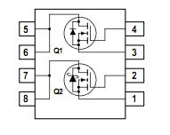 Specifications
| Symbol |
Parameter |
Q2 |
Q1 |
Units |
| VDSS |
Drain-Source Voltage |
30 |
30 |
V |
| VGSS |
Gate-Source Voltage |
±20 |
±16 |
V |
| ID |
Drain Current - Continuous (Note 1a)
- Pulsed |
8.6 |
6.3 |
A |
| 30 |
20 |
| PD |
Power Dissipation for Dual Operation |
2 |
W |
|
Power Dissipation for Single Operation
(Note 1a)
(Note 1b)
(Note 1c) |
1.6 |
| 1 |
| 0.9 |
| TJ, TSTG |
Operating and Storage Junction Temperature Range |
-55 to +150 |
°C |
DescriptionThe FDS6982S is designed to replace two single SO-8 MOSFETs and Schottky diode in synchronous DC:DC power supplies that provide various peripheral voltages for notebook computers and other battery powered electronic devices. FDS6982S contains two unique 30V, N-channel, logic level, PowerTrench MOSFETs designed to maximize power conversion efficiency.
The FDS6982S high-side switch (Q1) is designed with specific emphasis on reducing switching losses while the low- side switch (Q2) is optimized to reduce conduction losses. Q2 also includes an integrated Schottky diode using Fairchild's monolithic SyncFET technology.
Parameters: | Technical/Catalog Information | FDS6982S |
| Vendor | Fairchild Semiconductor |
| Category | Discrete Semiconductor Products |
| Mounting Type | Surface Mount |
| FET Polarity | 2 N-Channel (Dual) |
| Drain to Source Voltage (Vdss) | 30V |
| Current - Continuous Drain (Id) @ 25° C | 6.3A, 8.6A |
| Rds On (Max) @ Id, Vgs | 28 mOhm @ 6.3A, 10V |
| Input Capacitance (Ciss) @ Vds | 2040pF @ 10V |
| Power - Max | 900mW |
| Packaging | Tape & Reel (TR) |
| Gate Charge (Qg) @ Vgs | 12nC @ 5V |
| Package / Case | SO-8 |
| FET Feature | Logic Level Gate |
| Lead Free Status | Lead Free |
| RoHS Status | RoHS Compliant |
| Other Names | FDS6982S
FDS6982S
|

 FDS6982S Data Sheet