Configuration
: Single
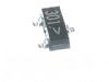
Mounting Style
: SMD/SMT
Packaging
: Reel
Transistor Polarity
: P-Channel
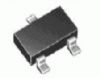
Package / Case
: SOT-23
Maximum Operating Temperature
: + 150 C
Drain-Source Breakdown Voltage
: - 25 V
Gate-Source Breakdown Voltage
: - 8 V
Continuous Drain Current
: 0.12 A
Resistance Drain-Source RDS (on)
: 13 Ohms
Features: -25 V, -0.12 A continuous, -0.5 A Peak.
RDS(ON) = 13@ VGS= -2.7 V
RDS(ON) = 10@ VGS= -4.5 V
Very low level gate drive requirements allowing direct operation in 3V circuits. VGS(th) < 1.5V.
Gate-Source Zener for ESD ruggedness.>6kV Human Body Model
Compact industry standard SOT-23 surface mount package.
Replace many PNP digital transistors (DTCx and DCDx) with one DMOS FET.
Pinout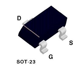 Specifications
| Symbol |
Parameter |
FDV302P |
Units |
VDSS
|
Drain-Source Voltage |
-25 |
V |
VGSS
|
Gate-Source Voltage |
-8 |
V |
ID
|
Drain Current - Continuous - Pulsed |
-0.12 |
A |
| -0.5 |
| PD |
Maximum Power Dissipation |
0.35 |
W |
TJ,TSTG
|
Operating and Storage Temperature Range |
-55 to 150 |
°C |
| ESD |
Electrostatic Discharge Rating MIL-STD-883D
Human Body Model (100pf / 1500 Ohm) |
6.0 |
kV |
DescriptionThis FDV302P P-Channel logic level enhancement mode field effect transistor is produced using Fairchild's proprietary, high cell density, DMOS technology. This very high density process is especially tailored to minimize on-state resistance. This device FDV302P has been designed especially for low voltage applications as a replacement for digital transistors. Since bias resistors are not required, this one P-channel FET can replace several digital transistors with different bias resistors such as the DTCx and DCDx series.
Parameters: | Technical/Catalog Information | FDV302P |
| Vendor | Fairchild Semiconductor |
| Category | Discrete Semiconductor Products |
| Mounting Type | Surface Mount |
| FET Polarity | P-Channel |
| Drain to Source Voltage (Vdss) | 25V |
| Current - Continuous Drain (Id) @ 25° C | 120mA |
| Rds On (Max) @ Id, Vgs | 10 Ohm @ 200mA, 4.5V |
| Input Capacitance (Ciss) @ Vds | 11pF @ 10V |
| Power - Max | 350mW |
| Packaging | Tape & Reel (TR) |
| Gate Charge (Qg) @ Vgs | 0.31nC @ 4.5V |
| Package / Case | SOT-23 |
| FET Feature | Standard |
| Lead Free Status | Lead Free |
| RoHS Status | RoHS Compliant |
| Other Names | FDV302P
FDV302P
FDV302PTR ND
FDV302PTRND
FDV302PTR
|

 FDV302P Data Sheet