FIN1025

Features: • Greater than 400Mbs data rate• Flow-through pinout simplifies PCB layout• 3.3V power supply operation• 0.4ns maximum differential pulse skew• 1.7ns maximum propagation delay• Low power dissipation• Power-Off protection• Meets or exceeds t...

product image

FIN1025 Picture
SeekIC No. : 004341614 Detail

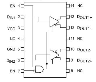
FIN1025: Features: • Greater than 400Mbs data rate• Flow-through pinout simplifies PCB layout• 3.3V power supply operation• 0.4ns maximum differential pulse skew• 1.7ns maximum ...

floor Price/Ceiling Price

Part Number:
FIN1025
Supply Ability:
5000

Price Break

  • Qty
  • 1~5000
  • Unit Price
  • Negotiable
  • Processing time
  • 15 Days
Total Cost: $ 0.00

SeekIC Buyer Protection PLUS - newly updated for 2013!

  • Escrow Protection.
  • Guaranteed refunds.
  • Secure payments.
  • Learn more >>

Month Sales

268 Transactions

Rating

evaluate  (4.8 stars)

Upload time: 2024/3/28

Payment Methods

All payment methods are secure and covered by SeekIC Buyer Protection PLUS.

Notice: When you place an order, your payment is made to SeekIC and not to your seller. SeekIC only pays the seller after confirming you have received your order. We will also never share your payment details with your seller.
Product Details

Description


Features:

• Greater than 400Mbs data rate
• Flow-through pinout simplifies PCB layout
• 3.3V power supply operation
• 0.4ns maximum differential pulse skew
• 1.7ns maximum propagation delay
• Low power dissipation
• Power-Off protection
• Meets or exceeds the TIA/EIA-644 LVDS standard
• 14-Lead TSSOP package saves space


Pinout

  Connection Diagram


Specifications

Supply Voltage (VCC)..................................... −0.5V to +4.6V
LVTTL DC Input Voltage (VIN)........................... −0.5V to +6V
LVDS DC Output Voltage (VOUT)..................... −0.5V to 4.6V
Driver Short Circuit Current (IOSD) .....................Continuous
Storage Temperature Range (TSTG) .......−65°C to +150°C
Max Junction Temperature (TJ) ..................................150°C
Lead Temperature (TL) ..............................................260°C
(Soldering, 10 seconds)
ESD (Human Body Model) ........................................10,000V
ESD (Machine Model) ....................................................600V


Description

This dual driver of FIN1025 is designed for high speed interconnects utilizing Low Voltage Differential Signaling (LVDS) technology.The driver translates LVTTL signal levels to LVDS levels with a typical differential output swing of 350mV which provides low EMI at ultra low power dissipation even at high frequencies. FIN1025 is ideal for high speed transfer of clock and data.

The FIN1025 can be paired with its companion receiver,the FIN1026, or any other LVDS receiver.


Customers Who Bought This Item Also Bought

Margin,quality,low-cost products with low minimum orders. Secure your online payments with SeekIC Buyer Protection.
Cables, Wires
Resistors
Motors, Solenoids, Driver Boards/Modules
Prototyping Products
DE1
Soldering, Desoldering, Rework Products
View more