FPGA

Features: • Second generation ASIC replacement technology - Densities as high as 5,292 logic cells with up to 200,000 system gates - Streamlined features based on Virtex architecture - Unlimited reprogrammability - Very low cost• System level features - SelectRAM+™ hierarchical m...

product image

FPGA Picture
SeekIC No. : 004343059 Detail

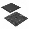
FPGA: Features: • Second generation ASIC replacement technology - Densities as high as 5,292 logic cells with up to 200,000 system gates - Streamlined features based on Virtex architecture - Unlimit...

floor Price/Ceiling Price

Part Number:
FPGA
Supply Ability:
5000

Price Break

  • Qty
  • 1~5000
  • Unit Price
  • Negotiable
  • Processing time
  • 15 Days
Total Cost: $ 0.00

SeekIC Buyer Protection PLUS - newly updated for 2013!

  • Escrow Protection.
  • Guaranteed refunds.
  • Secure payments.
  • Learn more >>

Month Sales

268 Transactions

Rating

evaluate  (4.8 stars)

Upload time: 2024/4/27

Payment Methods

All payment methods are secure and covered by SeekIC Buyer Protection PLUS.

Notice: When you place an order, your payment is made to SeekIC and not to your seller. SeekIC only pays the seller after confirming you have received your order. We will also never share your payment details with your seller.
Product Details

Description


Features:

• Second generation ASIC replacement technology
   - Densities as high as 5,292 logic cells with up to 200,000 system gates
   - Streamlined features based on Virtex architecture
   - Unlimited reprogrammability
   - Very low cost
• System level features
   - SelectRAM+™ hierarchical memory:
     · 16 bits/LUT distributed RAM
     · Configurable 4K bit block RAM
     · Fast interfaces to external RAM
   - Fully PCI compliant
   - Low-power segmented routing architecture
   - Full readback ability for verification/observability
   - Dedicated carry logic for high-speed arithmetic
   - Dedicated multiplier support
   - Cascade chain for wide-input functions
   - Abundant registers/latches with enable, set, reset
   - Four dedicated DLLs for advanced clock control
   - Four primary low-skew global clock distribution nets
   - IEEE 1149.1 compatible boundary scan logic
• Versatile I/O and packaging
   - Low cost packages available in all densities
   - Family footprint compatibility in common packages
   - 16 high-performance interface standards
   - Hot swap Compact PCI friendly
   - Zero hold time simplifies system timing
• Fully supported by powerful Xilinx development system
   - Foundation ISE Series: Fully integrated software
   - Alliance Series: For use with third-party tools
- Fully automatic mapping, placement, and routing


Specifications

Symbol Description
Min
Max
Units
VCCINT Supply voltage relative to GND(2)
0.5
3.0
V
VCCO Supply voltage relative to GND(2)
0.5
4.0
V
VREF Input reference voltage
0.5
3.6
V
VIN Input voltage relative to GND(3) 5V tolerant I/O(4)
0.5
5.5
V
No 5V tolerance(5)
0.5
VCCO+0.5
V
VTS Voltage applied to 3-state output 5V tolerant I/O(4)
0.5
5.5
V
No 5V tolerance(5)
0.5
VCCO+0.5
V
TSTG Storage temperature (ambient)
-6.5
+150
TJ Junction temperature
-
+125

Notes:
1. Stresses beyond those listed under Absolute Maximum Ratings may cause permanent damage to the device. These are stress ratings only, and functional operation of the device at these or any other conditions beyond those listed under Operating Conditions is not implied. Exposure to Absolute Maximum Ratings conditions for extended periods of time may affect device reliability.
2. Power supplies may turn on in any order.
3. VIN should not exceed VCCO by more than 3.6V over extended periods of time (e.g., longer than a day).
4. Spartan-II I/Os are 5V Tolerant whenever the LVTTL, LVCMOS2, or PCI33_5 signal standard has been selected. With 5V Tolerant I/Os selected, the Maximum DC overshoot must be limited to either +5.5V or 10 mA, and undershoot must be limited to either 0.5V or 10 mA, whichever is easier to achieve. The Maximum AC conditions are as follows: The device pins may undershoot to 2.0V or overshoot to +7.0V, provided this over/undershoot lasts no more than 11 ns with a forcing current no greater than 100 mA.
5. Without 5V Tolerant I/Os selected, the Maximum DC overshoot must be limited to either VCCO + 0.5V or 10 mA, and undershoot must be limited to 0.5V or 10 mA, whichever is easier to achieve. The Maximum AC conditions are as follows: The device pins may undershoot to 2.0V or overshoot to VCCO + 2.0V, provided this over/undershoot lasts no more than 11 ns with a forcing current no greater than 100 mA.
6. For soldering guidelines, see the Packaging Information on the Xilinx web site:
http://www.xilinx.com/publications/products/packaging/index.htm


Description

The Spartan™-II 2.5V Field-Programmable Gate Array FPGAs family gives users high performance, abundant logic resources, and a rich feature set, all at an exceptionally low price. The six-member family offers densities ranging from 15,000 to 200,000 system gates, as shown in Table 1. System performance is supported up to 200 MHz.

Spartan-II FPGAs family deliver more gates, I/Os, and features per dollar than other FPGAs by combining advanced process technology with a streamlined Virtex-based architecture. Features include block RAM (to 56K bits), distributed RAM (to 75,264 bits), 16 selectable I/O standards, and four DLLs. Fast, predictable interconnect means that successive design iterations continue to meet timing requirements.

The Spartan-II FPGAs family is a superior alternative to mask-programmed ASICs. The FPGA avoids the initial cost, lengthy development cycles, and inherent risk of conventional ASICs. Also, FPGA programmability permits design upgrades in the field with no hardware replacement necessary (impossible with ASICs).


Customers Who Bought This Item Also Bought

Margin,quality,low-cost products with low minimum orders. Secure your online payments with SeekIC Buyer Protection.
Cable Assemblies
Soldering, Desoldering, Rework Products
Semiconductor Modules
Line Protection, Backups
Transformers
View more