Features: ` Undershoot hardened to −2V (A and B Ports)
` Voltage level shifting
` 4 switch connection between two ports
` Minimal propagation delay through the switch
` Low lCC
` Zero bounce in flow-through mode
` Control inputs compatible with TTL level
` See Applications Note AN-5008 for details
` Also packaged in plastic Fine-Pitch Ball Grid Array (FBGA) (Preliminary)
ApplicationSelect pins S0, S1, S2 are intended to be used as static user configurable control pins. The AC performance of these pins has not been characterized or tested. Switching of these select pins during system operation may temporarily disrupt output logic states and/or enable pin controls.
Pinout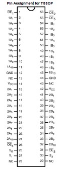 Specifications
Supply Voltage (VCC) ................................−0.5V to +7.0V
DC Switch Voltage (VS) (Note 3) ...............−2.0V to +7.0V
DC Input Control Pin Voltage
(VIN) (Note 4) ............................................−0.5V to +7.0V
DC Input Diode Current (lIK) VIN < 0V ...................−50 mA
DC Output (IOUT) Current ......................................128 mA
DC VCC/GND Current (ICC/IGND) .......................+/− 100 mA
Storage Temperature Range (TSTG) .........−65 to +150
Power Supply Operating (VCC) ........................4.0V to 5.5V
Input Voltage (VIN) .............................................0V to 5.5V
Output Voltage (VOUT) ........................................0V to 5.5V
Free Air Operating Temperature (TA) ...........-40 to +85
Note 2: The "Absolute Maximum Ratings" are those values beyond which the safety of the device cannot be guaranteed. The device should not be operated at these limits. The parametric values defined in the Electrical Characteristics tables are not guaranteed at the absolute maximum rating.
The "Recommended Operating Conditions" table will define the conditions for actual device operation.
Note 3: VS is the voltage observed/applied at either the A or B Ports across the switch.
Note 4: The input and output negative voltage ratings may be exceeded if the input and output diode current ratings are observed.
Note 5: Unused control inputs must be held HIGH or LOW. They may not float.
DescriptionThe Fairchild Universal Bus Switch FSTUD16450 provides 4-bit, 5-bit, 8-bit, 10-bit, 16-bit, 20-bit of high-speed CMOS TTL-compatible bus switching. The low On Resistance of the switch allows inputs to be connected to outputs without adding propagation delay or generating additional ground bounce noise.
The FSTUD16450 is designed to allow "customer" configuration control of the enable connections. The device is organized as either a 4-bit, 5-bit, 10-bit or 20-bit bus switch.
8-bit and 16-bit configurations are also achievable (see Functional Description). The FSTUD16450's bit configuration is chosen through select pin logic. (see Truth Table). When OEx is LOW, Port Ax is connected to Port Bx. When OEx is HIGH, the switch is OPEN.
The A and B Ports of FSTUD16450 are "undershoot hardened" with UHC protection to support an extended range to 2.0V below ground. Fairchild's integrated "Undershoot Hardened Circuit" (UHC) senses undershoot at the I/O's, and responds by preventing voltage differentials from developing and turning on the switch.
Another key FSTUD16450 feature is the addition of a level shifting select pin, "S2". When S2 is LOW, the device behaves as a standard N-MOS switch. When S2 is HIGH, a diode to VCC is integrated into the circuit allowing for level shifting between 5V inputs and 3.3V outputs.

 FSTUD16450 Data Sheet