Features: •FT pin for user-configurable flow through or pipeline
operation
• Single Cycle Deselect (SCD) operation
• 3.3 V +10%/5% core power supply
• 2.5 V or 3.3 V I/O supply
• LBO pin for Linear or Interleaved Burst mode
• Internal input resistors on mode pins allow floating mode pins
• Default to Interleaved Pipeline mode
• Byte Write (BW) and/or Global Write (GW) operation
• Common data inputs and data outputs
• Clock Control, registered, address, data, and control
• Internal self-timed write cycle
• Automatic power-down for portable applications
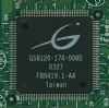
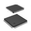
• JEDEC-standard 100-lead TQFP or QFP packageApplicationThe GS81032A is a 1,048,576-bit high performance synchronous SRAM with a 2-bit burst address counter. Although of a type originally developed for Level 2 Cache applications supporting high performance CPUs, the device now finds application in synchronous SRAM applications, ranging from DSP main store to networking chip set support.
Pinout Specifications
| Symbol |
Description |
Value |
Unit |
| VDD |
Voltage on VDD Pins |
0.5 to 4.6 |
V |
| VDDQ |
Voltage in VDDQ Pins |
0.5 to VDD |
V |
| VCK |
Voltage on Clock Input Pin |
-0.5 to 6 |
V |
| VI/O |
Voltage on I/O Pins |
0.5 to VDDQ+0.5 ( 4.6 V max.) |
V |
| VIN |
Voltage on Other Input Pins |
0.5 to VDD+0.5 ( 4.6 V max.) |
V |
| IIN |
Input Current on Any Pin |
+/20 |
mA |
| IOUT |
Output Current on Any I/O Pin |
+/20 |
mA |
| PD |
Package Power Dissipation |
1.5 |
W |
| TSTG |
Storage Temperature |
55 to 125 |
|
| TBIAS |
Temperature Under Bias |
55 to 125 |
|
Note:
Permanent damage to the device may occur if the Absolute Maximum Ratings are exceeded. Operation should be restricted to Recommended Operating Conditions. Exposure to conditions exceeding the Absolute Maximum Ratings, for an extended period of time, may affect reliability of this component.
DescriptionThe GS81032A is a 1,048,576-bit high performance synchronous SRAM with a 2-bit burst address counter. Although of a type originally developed for Level 2 Cache applications supporting high performance CPUs, the GS81032A now finds application in synchronous SRAM applications, ranging from DSP main store to networking chip set support.

 GS81032ATG Data Sheet