GS8182S18D-267

Features: • Simultaneous Read and Write SigmaQuad™ Interface• JEDEC-standard pinout and package• Dual Double Data Rate interface• Byte Write controls sampled at data-in time• DLL circuitry for wide output data valid window and future frequency scaling• Bur...

product image

GS8182S18D-267 Picture
SeekIC No. : 004355923 Detail

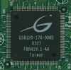
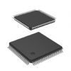
GS8182S18D-267: Features: • Simultaneous Read and Write SigmaQuad™ Interface• JEDEC-standard pinout and package• Dual Double Data Rate interface• Byte Write controls sampled at data-in...

floor Price/Ceiling Price

Part Number:
GS8182S18D-267
Supply Ability:
5000

Price Break

  • Qty
  • 1~5000
  • Unit Price
  • Negotiable
  • Processing time
  • 15 Days
Total Cost: $ 0.00

SeekIC Buyer Protection PLUS - newly updated for 2013!

  • Escrow Protection.
  • Guaranteed refunds.
  • Secure payments.
  • Learn more >>

Month Sales

268 Transactions

Rating

evaluate  (4.8 stars)

Upload time: 2024/5/6

Payment Methods

All payment methods are secure and covered by SeekIC Buyer Protection PLUS.

Notice: When you place an order, your payment is made to SeekIC and not to your seller. SeekIC only pays the seller after confirming you have received your order. We will also never share your payment details with your seller.
Product Details

Description


Features:

• Simultaneous Read and Write SigmaQuad™ Interface
• JEDEC-standard pinout and package
• Dual Double Data Rate interface
• Byte Write controls sampled at data-in time
• DLL circuitry for wide output data valid window and future frequency scaling
• Burst of 2 Read and Write
• 1.8 V +150/100 mV core power supply
• 1.5 V or 1.8 V HSTL Interface
• Pipelined read operation
• Fully coherent read and write pipelines
• ZQ mode pin for programmable output drive strength
• IEEE 1149.1 JTAG-compliant Boundary Scan
• 165-bump, 13 mm x 15 mm, 1 mm bump pitch BGA package
• RoHS-compliant 165-bump BGA package available
• Pin-compatible with future 36Mb, 72Mb, and 144Mb devices


Specifications

Symbol Description Value Unit
VDD Voltage on VDD Pins 0.5 to 2.9 V
VDDQ Voltage in VDDQ Pins 0.5 to VDD V
VI/O Voltage on I/O Pins 0.5 to VDDQ +0.5 ( 2.9 V max.) V
VIN Voltage on Other Input Pins 0.5 to VDDQ +0.5 ( 2.9 V max.) V
IIN Input Current on Any Pin +/100 mA dc
IOUT Output Current on Any I/O Pin +/100 mA dc
TJ Maximum Junction Temperature 125 °C
TSTG Storage Temperature 55 to 125 °C
TSUB Storage Under Bias 50 to 100 °C
VREF Voltage in VREF Pins 0.5 to VDDQ V

Note:
Permanent damage to the device may occur if the Absolute Maximum Ratings are exceeded. Operation should be restricted to Recommended Operating Conditions. Exposure to conditions exceeding the Recommended Operating Conditions, for an extended period of time, may affect reliability of this component.


Description

GS8182S18 are built in compliance with the SigmaSIO-II SRAM pinout standard for Separate I/O synchronous SRAMs. GS8182S18D-267 are 18,874,368-bit (18Mb) SRAMs. These are the first in a family of wide, very low voltage HSTL I/O SRAMs designed to operate at the speeds needed to implement economical high performance networking systems.


Customers Who Bought This Item Also Bought

Margin,quality,low-cost products with low minimum orders. Secure your online payments with SeekIC Buyer Protection.
Cables, Wires
Potentiometers, Variable Resistors
Test Equipment
Cables, Wires - Management
Resistors
View more