GTLP6C816A

Features: Interface between LVTTL and GTLP logic levels Edge Rate Control to minimize noise on the GTLP port Power up/down high impedance for live insertion1:6 fanout clock driver for LVTTL port1:2 fanout clock driver for GTLP portLVTTL compatible driver and control inputs Flow through pinout opti...

product image

GTLP6C816A Picture
SeekIC No. : 004357124 Detail

GTLP6C816A: Features: Interface between LVTTL and GTLP logic levels Edge Rate Control to minimize noise on the GTLP port Power up/down high impedance for live insertion1:6 fanout clock driver for LVTTL port1:2 ...

floor Price/Ceiling Price

Part Number:
GTLP6C816A
Supply Ability:
5000

Price Break

  • Qty
  • 1~5000
  • Unit Price
  • Negotiable
  • Processing time
  • 15 Days
Total Cost: $ 0.00

SeekIC Buyer Protection PLUS - newly updated for 2013!

  • Escrow Protection.
  • Guaranteed refunds.
  • Secure payments.
  • Learn more >>

Month Sales

268 Transactions

Rating

evaluate  (4.8 stars)

Upload time: 2024/4/30

Payment Methods

All payment methods are secure and covered by SeekIC Buyer Protection PLUS.

Notice: When you place an order, your payment is made to SeekIC and not to your seller. SeekIC only pays the seller after confirming you have received your order. We will also never share your payment details with your seller.
Product Details

Description


Features:

Interface between LVTTL and GTLP logic levels
Edge Rate Control to minimize noise on the GTLP port
Power up/down high impedance for live insertion
1:6 fanout clock driver for LVTTL port
1:2 fanout clock driver for GTLP port
LVTTL compatible driver and control inputs
Flow through pinout optimizes PCB layout
Open drain on GTLP to support wired-or connection
A Port source/sink −24/+24 mA
B Port sink 50 mA
−40 to +85 temperature capability
Low voltage version of GTLP6C816


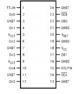
Pinout

  Connection Diagram


Specifications

Supply Voltage (VCC) ..............................−0.5V to +4.6V
DC Input Voltage (VI) ..............................−0.5V to +4.6V
DC Output Voltage (VO)
Outputs 3-STATE....................................  −0.5V to +4.6V
Outputs Active (Note 2)........................   −0.5V to +4.6V
DC Output Sink Current into
OA-Port IOL........................................................ . 48 mA
DC Output Source Current
from OA-Port IOH ...............................................−48 mA
DC Output Sink Current into
OB-Port in the LOW State IOL ............................100 mA
DC Input Diode Current (IIK)
VI< 0V ................................................................−50 mA
DC Output Diode Current (IOK)
VO < 0V ..............................................................−50 mA
VO > VCC..........................................................  +50 mA
ESD Rating ........................................................> 2000V
Storage Temperature (TSTG) ................−65 to +150


Description

The GTLP6C816A is a clock driver that provides LVTTL toGTLP signal level translation (and vice versa). The GTLP6C816A provides a high speed interface between cards operating atLVTTL logic levels and a backplane operating at GTL(P)logic levels. High speed backplane operation is a directresult of GTL(P)'s reduced output swing (<1V), reducedinput threshold levels and output edge rate control. Theedge rate control minimizes bus settling time. GTLP is a
Fairchild Semiconductor derivative of the Gunning Trans-ceiver logic (GTL) JEDEC standard JESD8-3.Fairchild's GTL(P) has internal edge-rate control and isprocess, voltage, and temperature (PVT) compensated. Itsfunction is similar to BTL and GTL but with different outputlevels and receiver threshold. GTLP  GTLP6C816A output LOW level istypically less than 0.5V, the output level HIGH is 1.5V andthe receiver threshold is 1.0V.


Customers Who Bought This Item Also Bought

Margin,quality,low-cost products with low minimum orders. Secure your online payments with SeekIC Buyer Protection.
View more