GTLPH16612

Features: • 18-bit bidirectional bus interface• Translates between GTLP logic levels (B ports) and LVTTL/TTL logic levels (A ports)• Edge rate control circuitry on the Bn outputs rising/falling edges to minimize system noise in a multipoint backplane environment• 5 V I/O to...

product image

GTLPH16612 Picture
SeekIC No. : 004357127 Detail

GTLPH16612: Features: • 18-bit bidirectional bus interface• Translates between GTLP logic levels (B ports) and LVTTL/TTL logic levels (A ports)• Edge rate control circuitry on the Bn outputs r...

floor Price/Ceiling Price

Part Number:
GTLPH16612
Supply Ability:
5000

Price Break

  • Qty
  • 1~5000
  • Unit Price
  • Negotiable
  • Processing time
  • 15 Days
Total Cost: $ 0.00

SeekIC Buyer Protection PLUS - newly updated for 2013!

  • Escrow Protection.
  • Guaranteed refunds.
  • Secure payments.
  • Learn more >>

Month Sales

268 Transactions

Rating

evaluate  (4.8 stars)

Upload time: 2024/4/30

Payment Methods

All payment methods are secure and covered by SeekIC Buyer Protection PLUS.

Notice: When you place an order, your payment is made to SeekIC and not to your seller. SeekIC only pays the seller after confirming you have received your order. We will also never share your payment details with your seller.
Product Details

Description


Features:

• 18-bit bidirectional bus interface
• Translates between GTLP logic levels (B ports) and LVTTL/TTL logic levels (A ports)
• Edge rate control circuitry on the Bn outputs rising/falling edges to minimize system noise in a multipoint backplane environment
• 5 V I/O tolerant on the LVTTL side
• No bus current loading when LVTTL output is tied to 5 V bus
• 3-State buffers
• Output capability: +64 mA/-32 mA on the LVTTL side; +40 mA on the GTLP side
• LVTTL input levels on control pins
• Power-up reset
• Power-up 3-State
• Positive edge triggered clock inputs
• Latch-up protection exceeds 500 mA per JESD78
• ESD protection exceeds 2000 V HBM per JESD22-A114,200 V MM per JESD22-A115 and 750 V (Bn I/O exceeds 1000 V) CDM per JESD22-C101


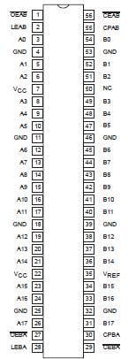
Pinout

  Connection Diagram


Specifications

SYMBOL
PARAMETER
CONDITIONS
RATING
UNIT
VCC
DC supply voltage  
0.5 to +4.6
V
IIK
DC input diode current VI < 0 V
-50
mA
VI
DC input voltage3 A port
0.5 to +7.0
V
B port
0.5 to +4.6
V
IOK
DC output diode current VO < 0 V; A port
-50
mA
VOUT
DC output voltage3 Output in Off or High state; A port
0.5 to +7.0
V
Output in Off or High state; B port
0.5 to +4.6
V
IOL
Current into any output in the LOW state A port
128
mA
B port
80
mA
IOH
Current into any output in the HIGH state A port
-64
mA
Tstg
Storage temperature range  
65 to +150
°C

1. Stresses beyond those listed may cause permanent damage to the device. These are stress ratings only and functional operation of the device at these or any other conditions beyond those indicated under "recommended operating conditions" is not implied. Exposure to absolute-maximum-rated conditions for extended periods may affect device reliability.
2. The performance capability of a high-performance integrated circuit in conjunction with its thermal environment can create junction temperatures which are detrimental to reliability. The maximum junction temperature of this integrated circuit should not exceed 150 °C.
3. The input and output negative voltage ratings may be exceeded if the input and output clamp current ratings are observed.


Description

The GTLPH16612 is a high-performance BiCMOS product designed for VCC operation at 3.3V with I/O compatibility up to 5 V.

The GTLPH16612 is unique in that pin 50 is a no connect and this device can be used as a replacement device in sockets where pin 50 is 3.3/5 V VCC or 3.3 V BIAS VCC.

GTLPH16612 is an 18-bit universal transceiver featuring non-inverting 3-State bus compatible outputs in both send and receive directions.Data flow in each direction is controlled by output enable (OEAB and OEBA), latch enable (LEAB and LEBA), and clock (CPAB and CPBA) inputs. For A-to-B data flow, the device operates in the transparent mode when LEAB is High. When LEAB is Low, the A data is latched if CPAB is held at a High or Low logic level. If LEAB is Low, the A-bus data is stored in the latch/flip-flop on the Low-to-High transition of CPAB. When OEAB is Low, the outputs are active. When OEAB is High, the outputs are in the high-impedance state. The clocks of GTLPH16612 can be controlled with the clock-enable inputs (CEBA/CEAB).Data flow for B-to-A is similar to that of A-to-B but uses OEBA,LEBA and CPBA.


Customers Who Bought This Item Also Bought

Margin,quality,low-cost products with low minimum orders. Secure your online payments with SeekIC Buyer Protection.
Power Supplies - Board Mount
Soldering, Desoldering, Rework Products
RF and RFID
Motors, Solenoids, Driver Boards/Modules
Prototyping Products
DE1
LED Products
View more