Features: • Zero Bus Latency, no dead cycles between write and read cycles
• Fast clock speed: 143, 133, 117, and 100MHz
• Fast access time: 4.0, 4.2, 4.5, 5.0ns
• Internally synchronized registered outputs eliminate the need to control OE#
• Single 3.3V -5% and +5% power supply
• Single R/W# (READ/WRITE) control pin
• Positive clock-edge triggered, address, data, and control signal registers for fully pipelined applications
• Interleaved or linear 4-word burst capability
• Individual byte write (BWa# - BWd#) control (may be tied LOW)
• CKE# pin to enable clock and suspend operations
• Three chip enables for simple depth expansion
• SNOOZE MODE for low power standby
• Automatic power down
• Packaged in a JEDEC standard 100-pin TQFP package
Pinout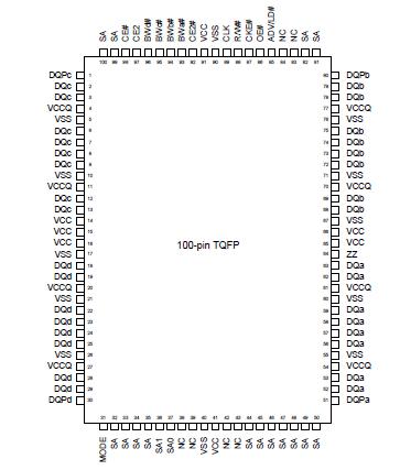 Specifications
Voltage on VCC Supply Relative to VSS........-0.5V to +4.6V
VIN .........................................................-0.5V to VCC+0.5V
Storage Temperature (plastic) ....................-55oC to +125o
Junction Temperature ................................................+125o
Power Dissipation ........................................................2.0W
Short Circuit Output Current .......................................50mA
DescriptionThe GVT71128ZC36 SRAM is designed to eliminatedead cycles when transitions from READ to WRITE or vice versa. This SRAM is optimized for 100 percent bus utilization and achieves Zero Bus Latency (ZBL). GVT71128ZC36 integrates 131,072x36 SRAM cells with advanced synchronous peripheral circuitry and a 2-bit counter for internal burst operation. The Galvantech Synchronous Burst SRAM family employs high-speed, low power CMOS designs using advanced triple-layer polysilicon, double-layer metal technology. Each memory cell consists of four transistors and two high valued resistors.
All synchronous inputs of GVT71128ZC36 are gated by registers controlled by a positive-edge-triggered clock input (CLK). The synchronous inputs include all addresses, all data inputs, depth-expansion chip enables (CE#, CE2# and CE2), cycle start input (ADV/LD#), clock enable (CKE#), byte write enables (BWa#, BWb#, BWc# and BWd#), and read-write control (R/W#).
Address and control signals of GVT71128ZC36 are applied to the SRAM during one clock cycle, and two cycles later, its associated data occurs, either read or write.
A clock enable (CKE#) pin allows operation of theGVT71128ZC36 to be suspended as long as necessary. Allsynchronous inputs are ignored when (CKE#) is high and the internal device registers will hold their previous values.
GVT71128ZC36 has three chip enable pins (CE#, CE2, CE2#) that allow the user to deselect the device when desired. If any one of these three are not active when ADV/LD# is low, no new memory operation of GVT71128ZC36 can be initiated and any burst cycle in progress is stopped. However, any pending data transfers (read or write) will be completed. The data bus will be in high impedance state two cycles after chip is deselected or a writecycle is initiated.
The GVT71128ZC36 has an on-chip 2-bit burst counter. In the burst mode, the GVT71128ZC36 provides four cycles of data for a single address presented to the SRAM. The order of the burst sequence is defined by the MODE input pin. The MODE pin selects between linear and interleaved burst sequence. The ADV/LD# signal is used to load a new external address (ADV/LD#=LOW) or increment the internal burst counter (ADV/LD#=HIGH)
Output enable (OE#), snooze enable (ZZ) and burst sequence select of GVT71128ZC36 (MODE) are the asynchronous signals. OE# can be used to disable the outputs at any given time. ZZ may be tied to LOW if it is not used.
The GVT71128ZC36 utilizes high performance high volume 3.3V CMOS process, and is packaged in a JEDEC Standard 14mm x 20mm 100-pin thin plastic quad flatpack (TQFP) for high board density.

 GVT71128ZC36 Data Sheet