Features: • Fast access times: 2.5 ns, 3.0 ns, and 3.5 ns
• Fast clock speed: 225 MHz, 200 MHz, 166 MHz, and 150 MHz
• Fast OE access times: 2.5 ns, 3.0 ns, and 3.5 ns
• Optimal for performance (two cycle chip deselect, depth expansion without wait state)
• 3.3V 5% and +10% power supply
• 3.3V or 2.5V I/O supply
• 5V tolerant inputs except I/Os
• Clamp diodes to VSS at all inputs and outputs
• Common data inputs and data outputs
• Byte Write Enable and Global Write control
• Multiple chip enables for depth expansion:three chip enables for TA(GVTI)/A(CY) package version and two chip enables for B(GVTI)/BG(CY) and T(GVTI)/AJ(CY) package versions
• Address pipeline capability
• Address, data and control registers
• Internally self-timed Write Cycle
• Burst control pins (interleaved or linear burst sequence)
• Automatic power-down for portable applications
• JTAG boundary scan for B and T package version
• Low profile 119-bump, 14-mm x 22-mm PBGA (Ball Grid Array) and 100-pin TQFP packages
Pinout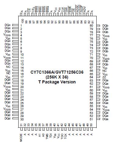 Specifications(Above which the useful life may be impaired. For user guidelines,not tested.)
Voltage on VCC Supply Relative to VSS ......... 0.5V to +4.6V
VIN ...........................................................0.5V to VCC+0.5V
Storage Temperature (plastic) .................55°C to +150°C
Junction Temperature ...............................................+150°C
Power Dissipation ......................................................... 1.0W
Short Circuit Output Current........................................ 50 mADescriptionThe Cypress Synchronous Burst SRAM CY7C1366A/GVT71256C36 family employs high-speed, low power CMOS designs using advanced triple-layer polysilicon, double-layer metal technology. Each memory cell consists of four transistors and two high valued resistors.
The CY7C1366A/GVT71256C36 and CY7C1367A/GVT71512C18 SRAMs integrate 262,144 x 36 and 524,288 x 18 SRAM cells with advanced synchronous peripheral circuitry and a 2-bit counter for internal burst operation. All synchronous inputs are gated by registers controlled by a positive-edge-triggered Clock Input (CLK). The synchronous inputs include all addresses, all data inputs, address-pipelining Chip Enable (CE), depth-expansion Chip Enables (CE2 and CE2), Burst Control Inputs of CY7C1366A/GVT71256C36 (ADSC, ADSP, and ADV), Write Enables (BWa, BWb, BWc, BWd, and BWE), and Global Write (GW). However, the CE2 Chip Enable input is only available for the TA(GVTI)/A(CY) package version.
Asynchronous inputs of CY7C1366A/GVT71256C36 include the Output Enable (OE) and Burst Mode Control (MODE). The data outputs (Q), enabled by OE, are also asynchronous.
Addresses and chip enables of CY7C1366A/GVT71256C36 are registered with either Address Status Processor (ADSP) or Address Status Controller (ADSC) input pins. Subsequent burst addresses can be internally generated as controlled by the Burst Advance Pin (ADV).Address, data inputs, and write controls are registered on-chip to initiate a self-timed WRITE cycle. WRITE cycles of CY7C1366A/GVT71256C36 can be one to four bytes wide, as controlled by the write control inputs.Individual byte write allows an individual byte to be written. BWa controls DQa. BWb controls DQb. BWc controls DQc.BWd controls DQd. BWa, BWb, BWc, and BWd can be active only with BWE being LOW. GW being LOW causes all bytes to be written. The x18 version only has 18 data inputs/outputs (DQa and DQb) along with BWa and BWb (no BWc, BWd,DQc, and DQd).
For the B(GVTI)/BG(CY) and T(GVTI)/AJ(CY) package versions,four pins of CY7C1366A/GVT71256C36 are used to implement JTAG test capabilities: Test Mode Select (TMS), Test Data-In (TDI), Test Clock (TCK), and Test Data-Out (TDO). The JTAG circuitry is used to serially shift data to and from the CY7C1366A/GVT71256C36. JTAG inputs use LVTTL/LVCMOS levels to shift data during this testing mode of operation. The TA package version does not offer the JTAG capability.
The CY7C1366A/GVT71256C36 and CY7C1367A/GVT71512C18 operate from a +3.3V power supply. All inputs and outputs are LVTTL compatible.

 GVT71256C36 Data Sheet