Features: • Fast access times: 2.5, and 3.5ns
• Fast clock speed: 250, 225, 200, and 166MHz
• 1ns setup time and hold time
• Fast OE# access times: 2.5ns and 3.5ns
• Optimal for depth expansion (one cycle chip deselect to eliminate bus contention)
• 3.3V -5% and +10% power supply
• 3.3V or 2.5V I/O supply
• 5V tolerant inputs except I/O's
• Clamp diodes to VSS at all inputs and outputs
• Common data inputs and data outputs
• BYTE WRITE ENABLE and GLOBAL WRITE control
• Three chip enables for depth expansion and address pipeline
• Address, data and control registers
• Internally self-timed WRITE CYCLE
• Burst control pins (interleaved or linear burst sequence)
• Automatic power-down for portable applications
• JTAG boundary scan
• JEDEC standard pinout
• Low profile 119 lead, 14mm x 22mm BGA (Ball Grid Array) and 100 pin TQFP packages
Pinout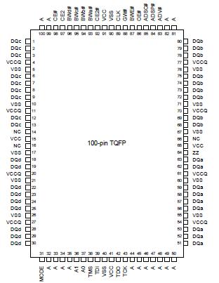 Specifications
Voltage on VCC Supply Relative to VSS........-0.5V to +4.6V
VIN .........................................................-0.5V to VCC+0.5V
Storage Temperature (plastic) ...................-55oC to +150o
Junction Temperature ...............................................+150o
Power Dissipation .......................................................1.0W
Short Circuit Output Current ......................................50mA
*Stresses greater than those listed uunder "Absolute Maximum Ratings" may cause permanent damage to the device.This is a stress rating only and functional operation of the device at these or any other conditions above those indicated in the operational sections of this specification is not implied. Exposure to absolute maximum rating conditions for extended periods may affect reliability.
DescriptionThe Galvantech Synchronous Burst SRAM GVT71128DA36 and GVT71256DA18 family employs high-speed, low power CMOS designs using advanced triple-layer polysilicon, double-layer metal technology. Each memory cell consists of four transistors and two high valued resistors.
The GVT71128DA36 and GVT71256DA18 SRAMs integrate 131,072x36 and 262,144x18 SRAM cells with advanced synchronous peripheral circuitry and a 2-bit counter for internal burst operation. All synchronous inputs are gated by registers controlled by a positive-edge-triggered clock input (CLK). The synchronous inputs of GVT71128DA36 and GVT71256DA18 include all addresses, all data inputs, address-pipelining chip enable (CE#), depthexpansion chip enables (CE2# and CE2), burst control inputs (ADSC#, ADSP#, and ADV#), write enables (BWa#, BWb#, BWc#, BWd#, and BWE#), and global write (GW#).
Asynchronous inputs of GVT71128DA36 and GVT71256DA18 include the output enable (OE#) and burst mode control (MODE). The data outputs (Q), enabled by OE#, are also asynchronous.
Addresses and chip enables of GVT71128DA36 and GVT71256DA18 are registered with either address status processor (ADSP#) or address status controller (ADSC#) input pins. Subsequent burst addresses can be internally generated as controlled by the burst advance pin (ADV#).
Address, data inputs, and write controls of GVT71128DA36 and GVT71256DA18 are registered onchip to initiate self-timed WRITE cycle. WRITE cycles can be one to four bytes wide as controlled by the write control inputs. Individual byte write allows individual byte to be written. BWa# controls DQa. BWb# controls DQb. BWc# controls DQc. BWd# controls DQd. BWa#, BWb# BWc#, and BWd# can be active only with BWE# being LOW. GW# being LOW causes all bytes to be written. The x18 version only has 18 data inputs/outputs (DQa and DQb) along with BWa# and BWb# (no BWc#, BWd#, DQc, and DQd). Four pins of GVT71128DA36 and GVT71256DA18 are used to implement JTAG test capabilities: test mode select (TMS), test data-in (TDI), test clock (TCK), and test data-out (TDO). The JTAG circuitry is used to serially shift data to and from the device. JTAG inputs of GVT71128DA36 and GVT71256DA18 use LVTTL/LVCMOS levels to shift data during this testing mode of operation.
The GVT71128DA36 and GVT71256DA18 operate from a +3.3V power supply. All inputs and outputs are LVTTL compatible

 GVT71256DA18 Data Sheet