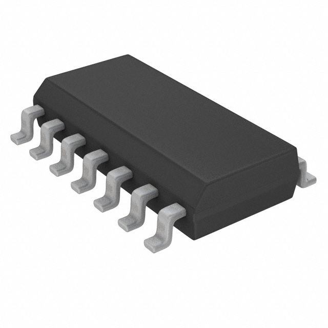
Pinout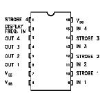
Specifications
| Symbol |
Parameter |
Value |
Unit |
| VDD* |
Supply Voltage :HCC Types
HCF Types |
0.5 to + 20
0.5 to + 18 |
V
V |
| Vi |
Input Voltage |
0.5 to V + 0.5 |
V |
| II |
DC Input Current (any one input) |
± 10 |
mA |
| Ptot |
Total Power Dissipation (per package)
Dissipation per Output Transistor
for Top = Full Package-temperature Range |
200
100 |
mW
mW |
| Top |
Operating Temperature : HCC Types
HCF Types |
55 to + 125
40to+85 |
°C
°C |
| Tstg |
Storage Temperature |
65 to + 150 |
°C |
DescriptionThe HCC4054B, HCC4055B and HCC4056B (extended temperature range) and the HCF4054B, HCF4055B and HCF4056B (intermediate temperaturerange)aremonolithicintegratedcircuitsavailable in16-lead dualin-lineplastic orceramic packageand plastic micro package. The HCC/HCF4055B and HCC/HCF4056B typesaresingle-digit BCD-to-7-seg-ment decoder/driver circuits that provide level-shifting functions on the chip. This feature permits the BCD input-signal swings(VDD toVSS) tobe thesame as ordifferentfromthe7-segmentoutput-signalswings (VDD to VEE). For example, the BCD input-signal swings (VDD to VSS) may be as low as 0 to 3V, whereasthe output-display drive-signal swing(VDD toVEE)maybefrom0to5V.IfVDD toVEEexceeds 15V,VDD to VSS should be atleast 4V.The 7-seg- ment outputsarecontrolled by theDISPLAY-FRE- QUENCY (DF) input which causes the selected segmentoutputsto below,high,or asquare-wave output (for liquid-crystal displays). When the DF inputis low the output segments will be highwhen selectedby the BCD inputs. When the DF input is high, theoutputsegmentswillbelowwhenselected by theBCDinputs. When asquare-wave ispresent at the DF input,the selected segments willhave a square-wave output thatis 180° outof phasewith the DF input. Those segments which are not se- lected will have a square-wave output that is in phase with the input. DF square-wave repetition rates for liquid-crystal displays usually range from 30Hz(wellabove flickerrate)to200Hz(wellbelow the upper limit of the liquid-crystal frequency response). The HCC/HCF4055B provides a levelshifted high-amplitude DF outputwhich is required for driving the common electrode in liquid-crystal displays. TheHCC/HCF4056Bprovides a strobed latch function at the BCD inputs. Decoding of all input combinations on the HCC/HCF4055B and HCC/HCF4056Bprovides displays of 0to 9aswell asL, P,H,A,,andablank position.(seetypicalapplication forother letters).TheHCC/HCF4054Bprovides level shifting similar to the HCC/HCF4055B and HCC/HCF4056Bindependently strobedlatches, and common DF control on 4 signal lines. The HCC/HCF4054Bisintended toprovide drive-signal compatibility with the HCC/HCF4055B and HCC/HCF4056B 7-segment decoder types for the decimalpoint,colon,polarity,andsimilardisplaylines. Alevel-shiftedhigh-amplitude DF output canbe obtainedfromany HCC/HCF4054B outputlinebyconnecting the corresponding inputand strobelinesto a low and high level, respectively. The HCC/HCF4054B mayalso beutilizedforlogic-level "upconversion"or"downconversion". Forexample, input-signal swings (VDD toVSS) from+5to 0V can beconvertedtooutput-signalswings(VDD toVEE)of + 5 to 5V. The level-shifted function on all three typespermits the use of differentinput-and outputsignalswings. The inputswingsfrom a lowlevel of VSS to a high level of VDD while the outputswings fromalowlevelofVEE tothesame highlevelofVDD. Thus,the inputand output swingscan be selected independently of each otherovera3-to-18V range. VSS may be connected to VEE when no level-shift function isrequired. For the HCC/HCF4054B and HCC/HCF4056B, dataaretransferredfrominput to outputbyplacing a high voltage levelat the strobe input.Alowvoltagelevelat thestrobeinput latches the data input and the corresponding output seg- ments remain selected (or non-selected) whilethe strobe is low.Whenever the level-shiftingfunction isrequired, the HCC/HCF4055B canbe usedbyit selfto drive a liquid-crystal display(fig. 10 and fig. 12).The HCC/HCF4056B, however,must be used together with a HCC/HCF4054B to providethecommon DF output(fig. 14).Thecapability of extending hevoltage swingon thenegative end(thisvoltage cannot be extended on the positive end) can be used to advantagein theset-upof fig.11. Fig.9 is commonto allthreetypes.

 HCF4054B Data Sheet