HCF4094BM1_1183347

PinoutSpecifications Symbol Parameter Value Unit VDD Supply Voltage -0.5 to +22 V VI DC Input Voltage -0.5 to VDD + 0.5 V II DC Input Current ± 10 mA PD Power Dissipation per Package 500(*) mW Power Dissipation per Output Transistor 100 mW Top Operating ...

product image

HCF4094BM1_1183347 Picture
SeekIC No. : 004359698 Detail

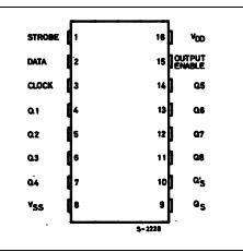
HCF4094BM1_1183347: PinoutSpecifications Symbol Parameter Value Unit VDD Supply Voltage -0.5 to +22 V VI DC Input Voltage -0.5 to VDD + 0.5 V II DC Input Current ± 10 mA PD Power Dissipa...

floor Price/Ceiling Price

Part Number:
HCF4094BM1_1183347
Supply Ability:
5000

Price Break

  • Qty
  • 1~5000
  • Unit Price
  • Negotiable
  • Processing time
  • 15 Days
Total Cost: $ 0.00

SeekIC Buyer Protection PLUS - newly updated for 2013!

  • Escrow Protection.
  • Guaranteed refunds.
  • Secure payments.
  • Learn more >>

Month Sales

268 Transactions

Rating

evaluate  (4.8 stars)

Upload time: 2024/5/5

Payment Methods

All payment methods are secure and covered by SeekIC Buyer Protection PLUS.

Notice: When you place an order, your payment is made to SeekIC and not to your seller. SeekIC only pays the seller after confirming you have received your order. We will also never share your payment details with your seller.
Product Details

Description


Pinout

  Connection Diagram


Specifications

Symbol Parameter Value Unit
VDD Supply Voltage -0.5 to +22 V
VI DC Input Voltage -0.5 to VDD + 0.5 V
II DC Input Current ± 10 mA
PD Power Dissipation per Package 500(*) mW
Power Dissipation per Output Transistor 100 mW
Top Operating Temperature -55 to +125
Tstg Storage Temperature -65 to +150

Absolute Maximum Ratings are those values beyond which damage to the device may occur. Functional operation under these conditions is not implied.
All voltage values are referred to VSS pin voltage.
(*) 500mW at 65 °C; derate to 300mW by 10mW/°Cfrom65°Cto85°C


Description

The HCF4094B is a monolithic integrated circuit fabricated in Metal Oxide Semiconductor technology available in DIP and SOP packages. The HCF4094B is an 8 stages serial shift register having a storage latch associated with each stage for strobing data from the serial input to parallel buffered 3-state outputs. The parallel outputs may be connected directly to common bus lines. Data is shifted on positive clock transition. The data in each shift register stage is transferred to the storage register when the STROBE input is high.Data in the storage register appears at the outputs whenever the OUTPUT-ENABLE signal is high.Two serial outputs are available for cascading a number of HCF4094B devices. Data is available at the QS serial output terminal on positive clock edges to allow for high speed operation in cascaded system in which the clock rise time is fast. The same serial nformation, available at the Q'S terminal on the next negative clock edge,provides a means for cascading HCF4094B devices when the clock rise time is slow.


Customers Who Bought This Item Also Bought

Margin,quality,low-cost products with low minimum orders. Secure your online payments with SeekIC Buyer Protection.
RF and RFID
Inductors, Coils, Chokes
Programmers, Development Systems
Memory Cards, Modules
Circuit Protection
Cables, Wires
View more