HDMP-0421

Features: • Supports ANSI X3T11 1.0625 Gbps FC-AL Loop Configuration• Supports 802.3z 1.25 Gbps Gigabit Ethernet (GE) Rates• Single PBC, CDR, Dual Signal Detect (SD) in a Single Package• Bidirectional, Symmetric Bypass Capability• CDR in Bypass Path and Loop Path̶...

product image

HDMP-0421 Picture
SeekIC No. : 004361028 Detail

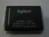
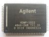
HDMP-0421: Features: • Supports ANSI X3T11 1.0625 Gbps FC-AL Loop Configuration• Supports 802.3z 1.25 Gbps Gigabit Ethernet (GE) Rates• Single PBC, CDR, Dual Signal Detect (SD) in a Single Pa...

floor Price/Ceiling Price

Part Number:
HDMP-0421
Supply Ability:
5000

Price Break

  • Qty
  • 1~5000
  • Unit Price
  • Negotiable
  • Processing time
  • 15 Days
Total Cost: $ 0.00

SeekIC Buyer Protection PLUS - newly updated for 2013!

  • Escrow Protection.
  • Guaranteed refunds.
  • Secure payments.
  • Learn more >>

Month Sales

268 Transactions

Rating

evaluate  (4.8 stars)

Upload time: 2024/4/27

Payment Methods

All payment methods are secure and covered by SeekIC Buyer Protection PLUS.

Notice: When you place an order, your payment is made to SeekIC and not to your seller. SeekIC only pays the seller after confirming you have received your order. We will also never share your payment details with your seller.
Product Details

Description


Features:

• Supports ANSI X3T11 1.0625 Gbps FC-AL Loop Configuration
• Supports 802.3z 1.25 Gbps Gigabit Ethernet (GE) Rates
• Single PBC, CDR, Dual Signal Detect (SD) in a Single Package
• Bidirectional, Symmetric Bypass Capability
• CDR in Bypass Path and Loop Path
• CDR Location Determined by Wiring Configuration of Pins on PCB (Patent Pending)
• Envelope Detect on Cable Input (SD) for Both Directions
• Equalizers On All Inputs
• High Speed PECL I/Os Referenced to VCC
• Buffered Line Logic (BLL) Outputs without External Bias Resistors
• 0.4 W Typical Power at VCC = 3.3 V
• 5 V Tolerant LVTTL I/O
• 24 Pin SSOP Package


Application

• RAID, JBOD Cabinets
• 1=>1 Gigabit Serial Buffer Pair (with and w/o CDR)
• Multi-Initiator Loops


Specifications

Symbol Parameter Units Min. Max.
VCC Supply Voltage V 0.7 4.0
VIN,LVTTL

VIN,HS_IN

IO,LVTTL
LVTTL Input Voltage

HS_IN Input Voltage

LVTTL Output Source Current
V

V

mA
0.7

2.0
4.0

VCC

± 13
Tstg

Tj
Storage Temperature

Junction Temperature


0.7

2.0
+150

+125


Description

The HDMP-0421 is a Single Port Bypass Circuit (PBC) with Clock and Data Recovery (CDR), and dual Signal Detect (SD) capability. This configuration will control jitter accumulation while repeating incoming signals. Port Bypass Circuits are used to provide loops that are continuously on in hard disk arrays constructed in Fibre Channel Arbitrated Loop (FC-AL) configurations. Hard disks may be pulled out or swapped while other disks in the array are available to the system. This device may also be used in multi-initiator loop configurations. A Port Bypass Circuit is a 2:1 Multiplexer array with two modes of operation: DISK IN LOOP and DISK BYPASSED. In DISK IN LOOP mode, the loop goes into and out of the disk drive. Data go from the HDMP-0421's TO_NODE[n]± differential output pins to the Disk Drive Transceiver IC (for example, an HDMP-1536A) Rx± differential input pins. Data from the Disk Drive Transceiver IC Tx± differential output pins go to the HDMP-0421's FM_NODE[n]± differential input pins. Figures 4 and 5 show connection diagrams for disk drive array applications.

In DISK BYPASSED mode, the disk drive is either absent or non-functional and the loop bypasses the hard disk. DISK IN LOOP mode is enabled with a HIGH on the BYPASS[n] pin and DISK BYPASSED mode is enabled with a LOW on the same pin. Multiple HDMP-0421s may be cascaded or connected to other members of the HDMP-04xx family through the FM_LOOP and TO_LOOP pins to create loops for arrays of disk drives. See Table 2 to identify which of the two cells (0:1) will provide FM_LOOP, TO_LOOP pins (cell connected to cable). ALL TO_NODE outputs of the HDMP-0421 are of equal strength. Combinations of HDMP-04xx may be utilized to accommodate any number of hard disks.

The HDMP-0421 may also be used as a pair of 1=>1 buffers, one with a CDR and another without. For example, HDMP-0421 may be placed in front of a CMOS ASIC to clean the jitter of the outgoing signal (CDR path) and to better read the incoming signal (CDRless path).


Customers Who Bought This Item Also Bought

Margin,quality,low-cost products with low minimum orders. Secure your online payments with SeekIC Buyer Protection.
Batteries, Chargers, Holders
Prototyping Products
DE1
Optoelectronics
View more