SeekIC No. : 004362528
Detail
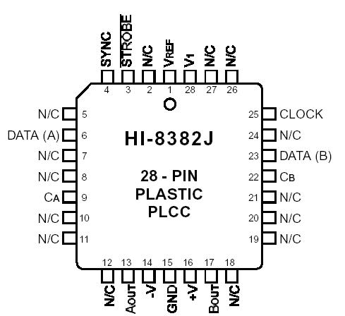
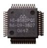
HI-8382: Features: ·Low power CMOS·TTL and CMOS compatible inputs·Programmable output voltage swing·Adjustable ARINC rise and fall times·Operates at data rates up to 100 Kbits·Overvoltage protection·Industri...
 HI-8382 Data Sheet
floor Price/Ceiling Price
- Part Number:
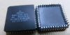
- HI-8382
- Supply Ability:
- 5000
Price Break
- Qty
- 1~5000
- Unit Price
- Negotiable
- Processing time
- 15 Days
SeekIC Buyer Protection PLUS - newly updated for 2013!
- Escrow Protection.
- Guaranteed refunds.
- Secure payments.
- Learn more >>
Month Sales
268 Transactions
Payment Methods
All payment methods are secure and covered by SeekIC Buyer Protection PLUS.
Notice: When you place an order, your payment is made to SeekIC and not to your seller. SeekIC only pays the seller after confirming you have received your order. We will also never share your payment details with your seller.