Features: • Six Channel MOSFET Driver with Gate Drive Control by Serial (SPI) or Parallel Interface and an Option for PWM Logic Switching Control
• Drain Monitor Provides Fault Detection and Voltage Clamp for Each Channel
• Output Voltage Zener Clamp. . . . . . . . . . 67V Typ
• 5V CMOS Logic Level Input Control
• VCC Logic Level Power Supply
- 5V VCC Logic Power Supply
- Turns Off Gate Drive for Low or Loss of VCC
• VPWR System Level Power Supply Management
- 5.5V to 17V Battery/System Level Power Supply Monitor
- Over-Voltage Shutdown. . . . . . . . . . . . 35V Typ
• Output Supply/Load Short and Open Load/Ground Short Fault Detection
• Automatic Change to Low Duty Cycle Drive Mode When Output Short-to-Supply Detected
• Fault Diagnostic Feedback via the SPI Bus
• Operating Temp Range . . . . . . . -40 to +125Application• Automotive and Industrial Systems
• Control of Solenoids, Relays and Lamp Drivers
• Interface to Logic and mP Controllers
• Robotic System ControllerPinout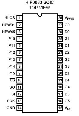 SpecificationsLogic Supply Voltage, VCC . . . . . . . . . . . . . . . . . . . . . . . -0.3V to 7V
Max Quiescent Logic Supply Current, ICC . . . . . . . . . . . . . . .. . .5mA
Logic Input Voltage . . . . . . . . . . . . . . . . . . . . . -0.3V to VCC + 0.3V
System Supply Voltage Monitor, VPWR (Note 1)
Max Continuous . . . . . . . . . . . . . . . . . . . . . . . . . . . .. .. -1.5V to 38V
Max Drain Clamp Voltage, VDM (Note 2) . . . . . . . .. . . . . . . . . . . 75V
Max Gate Drive Output Voltage, VG (Note 3) . . . .-0.3 to VCC + 0.3V
Operating Ambient Temperature Range, TA . . .. .. . .-40 to +125
Operating Junction Temperature Range . . . . . .. .. . .-40 to +150
Storage Temperature Range, TSTG . . . . . . . . . .. .. . -55 to +150
Lead Temperature (Soldering 10s Max) . . . . . . . . . . . . . . . +265DescriptionThe HIP0063 is a logic controlled, six channel Low Side Power Driver. As shown in the Block Diagram, the outputs are controlled via the serial data interface or, by user option, each output may be independently controlled from the respective parallel input. In addition, PWM logic switching control (HLOS) may be directly applied to channels 0 and 1 in parallel, or channels 4 and 5 in parallel.
Output fault conditions of HIP0063 may be detected as an output load short to supply when the output is ON or as an open load/ground short when the output is OFF. If an over-current short exists at one output, gate drive goes to a low duty cycle mode. HIP0063 will remain in the low duty cycle mode until switched off or the fault is cleared. Fault bits are sent to a fault register to indicate which channel is at fault. The fault bits are indicated by a logic one and is internally latched when CS goes low. A fault bit will return to zero when the fault disappears. Either an 8-bit or 16-bit SPI communication mode may be used. Refer to the application section for bit control information.
Over-voltage shutdown protection for all outputs will occur when VPWR (Battery/ MOSFET Supply) exceeds 35V typical. When VCC is less than 3.5V, gate drive is switched off. The input and gate control logic is fully function when the VCC supply is greater than 4V typical. The HIP0063 has an internal drain-to-gate zener which is used to voltage clamp the output drain-to-source voltage of the MOSFET.
The HIP0063 is fabricated in a Power BiMOS IC process, and is intended for use in automotive and other applications having a wide range of temperature and electrical stress conditions. It is particularly well suited for MOSFET control in circuits driving lamps, displays, relays, and solenoids in applications requiring low operating power.

 HIP0063 Data Sheet