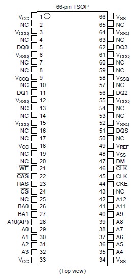
HM5425401B

Features: • 2.5 V power supply• SSTL-2 interface for all inputs and outputs• Clock frequency: 143 MHz/133 MHz/125 MHz/100 MHz (max)• Data inputs, outputs, and DM are synchronized with DQS• 4 banks can operate simultaneously and independently• Burst read/write op...

product image

HM5425401B Picture
SeekIC No. : 004363477 Detail

HM5425401B: Features: • 2.5 V power supply• SSTL-2 interface for all inputs and outputs• Clock frequency: 143 MHz/133 MHz/125 MHz/100 MHz (max)• Data inputs, outputs, and DM are synchron...

floor Price/Ceiling Price

Part Number:
HM5425401B
Supply Ability:
5000

Price Break

  • Qty
  • 1~5000
  • Unit Price
  • Negotiable
  • Processing time
  • 15 Days
Total Cost: $ 0.00

SeekIC Buyer Protection PLUS - newly updated for 2013!

  • Escrow Protection.
  • Guaranteed refunds.
  • Secure payments.
  • Learn more >>

Month Sales

268 Transactions

Rating

evaluate  (4.8 stars)

Upload time: 2024/5/4

Payment Methods

All payment methods are secure and covered by SeekIC Buyer Protection PLUS.

Notice: When you place an order, your payment is made to SeekIC and not to your seller. SeekIC only pays the seller after confirming you have received your order. We will also never share your payment details with your seller.
Product Details

Description


Features:

• 2.5 V power supply
• SSTL-2 interface for all inputs and outputs
• Clock frequency: 143 MHz/133 MHz/125 MHz/100 MHz (max)
• Data inputs, outputs, and DM are synchronized with DQS
• 4 banks can operate simultaneously and independently
• Burst read/write operation
• Programmable burst length: 2/4/8
--Burst read stop capability
• Programmable burst sequence
--Sequential
--Interleave
• Start addressing capability
--Even and Odd
• Programmable CAS latency: 2/2.5
• 8192 refresh cycles: 7.8 s (64 ms/8192 cycles)
• 2 variations of refresh
--Auto refresh
--Self refresh


Pinout

  Connection Diagram


Specifications

 Parameter  Symbol  Value  Unit  Note
 Supply voltage relative to VSS  VCC, VCCQ  1.0 to +3.6  V  
 Voltage on inputs pin relative to Vss  Vti  1.0 to +3.6  V  
 Voltage on I/O pins relative to VSS  VTio  0.5 to +3.6  V  
 Short circuit output current  Iout  50  mA  
 Power dissipation  PT  1.0  W  
 Operating temperature  Topr  0 to +70    
 Storage temperature  Tstg  -55 to +125    


Description

The HM5425161B, the HM5425801B and the HM5425401B are the Double Data Rate (DDR) SDRAM devices. Read and write operations are performed at the cross points of the CLK and the CLK . This high speed data transfer is realized by the 2-bit prefetch piplined architecture. Data strobe (DQS) both for read and write are available for high speed and reliable data bus design. By setting extended mode resistor, the on-chip Delay Locked Loop (DLL) can be set enable or disable.


Customers Who Bought This Item Also Bought

Margin,quality,low-cost products with low minimum orders. Secure your online payments with SeekIC Buyer Protection.
Audio Products
Optoelectronics
Potentiometers, Variable Resistors
Programmers, Development Systems
Semiconductor Modules
Cable Assemblies
View more