DescriptionThe HV03 and HV05 are low voltage serial to high voltage parallel converters with open drain outputs. These devices have been designed for use as drivers for AC-electroluminescent displays. They can also be used in any application requiring multiple output high voltage current sinking c...
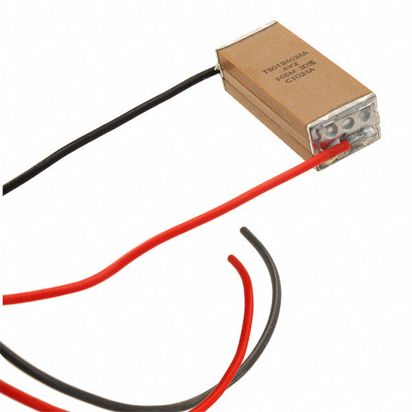
HV03: DescriptionThe HV03 and HV05 are low voltage serial to high voltage parallel converters with open drain outputs. These devices have been designed for use as drivers for AC-electroluminescent display...
SeekIC Buyer Protection PLUS - newly updated for 2013!
268 Transactions
All payment methods are secure and covered by SeekIC Buyer Protection PLUS.
The HV03 and HV05 are low voltage serial to high voltage parallel converters with open drain outputs. These devices have been designed for use as drivers for AC-electroluminescent displays. They can also be used in any application requiring multiple output high voltage current sinking capabilities such as driving inkjet and electrostatic print heads, plasma panels, vacuum fluorescent, or large matrix LCD displays. These devices consist of a 64-bit shift register, 64 latches, and control logic to perform the polarity select and blanking of the outputs. Data is shifted through the shift register on the high to low transition of the clock. The HV03 shifts in the counterclockwise direction when viewed from the top of the package and the HV05 shifts in the clockwise direction. A data output buffer is provided for cascading devices. This output reflects the current status of the last bit of the shift register. Operation of the shift register is not affected by the LE (latch enable), BL (blanking), or the POL (polarity) inputs. Transfer of data from the shift register to the latch occurs when the LE Each enable) input is high. The data in the latch is stored when LE is low. The HV03 and HV05 have been designed to be used in systems which either switch off the high voltage supply before changing the state of the high voltage outputs or limit the current through each output.
The features of HV03/HV05 can be summarized as (1)HVCMOS technology; (2)output voltages up to 300V using a ramped supply; (3)sink current minimum 100 mA; (4)shift register speed 8 MHz; (5)latched outputs; (6)output polarity and blanking; (7)CMOS compatible inputs; (8)forward and reverse shifting options.
The absolute maximum ratings of HV03/HV05 are (1)supply voltage, VDD: -0.5V to +15V; (2)supply voltage, VPP: -0.5V to +315V; (3)logic input levels: -0.5V to VDD +0.5V; (4)ground currents: 6.0A; (5)continuous total power dissipationt ceramic: 1900mW/Plastic: 1200mW; (6)operating temperature range commercial: -40°C to +85°C/military -55°C to +125°C; (7)storage temperature range: -65°C to 150°C.