HY27SS16121M

Features: · HIGH DENSITY NAND FLASH MEMORIES- Cost effective solutions for mass storage applications· NAND INTERFACE- x8 or x16 bus width.- Multiplexed Address/ Data- Pinout compatibility for all densities· SUPPLY VOLTAGE- 3.3V device: VCC = 2.7 to 3.6V : HY27USXX561M- 1.8V device: VCC = 1.7 to 1....

product image

HY27SS16121M Picture
SeekIC No. : 004368156 Detail

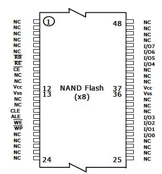
HY27SS16121M: Features: · HIGH DENSITY NAND FLASH MEMORIES- Cost effective solutions for mass storage applications· NAND INTERFACE- x8 or x16 bus width.- Multiplexed Address/ Data- Pinout compatibility for all de...

floor Price/Ceiling Price

Part Number:
HY27SS16121M
Supply Ability:
5000

Price Break

  • Qty
  • 1~5000
  • Unit Price
  • Negotiable
  • Processing time
  • 15 Days
Total Cost: $ 0.00

SeekIC Buyer Protection PLUS - newly updated for 2013!

  • Escrow Protection.
  • Guaranteed refunds.
  • Secure payments.
  • Learn more >>

Month Sales

268 Transactions

Rating

evaluate  (4.8 stars)

Upload time: 2024/5/3

Payment Methods

All payment methods are secure and covered by SeekIC Buyer Protection PLUS.

Notice: When you place an order, your payment is made to SeekIC and not to your seller. SeekIC only pays the seller after confirming you have received your order. We will also never share your payment details with your seller.
Product Details

Description


Features:

· HIGH DENSITY NAND FLASH MEMORIES
- Cost effective solutions for mass storage applications
· NAND INTERFACE
- x8 or x16 bus width.
- Multiplexed Address/ Data
- Pinout compatibility for all densities
· SUPPLY VOLTAGE
- 3.3V device: VCC = 2.7 to 3.6V : HY27USXX561M
- 1.8V device: VCC = 1.7 to 1.95V : HY27SSXX561M
· Memory Cell Array
- 256Mbit = 528 Bytes x 32 Pages x 2,048 Blocks
· PAGE SIZE
- x8 device : (512 + 16 spare) Bytes
: HY27US08561M
- x16 device: (256 + 8 spare) Words
: HY27US16561M
· BLOCK SIZE
- x8 device: (16K + 512 spare) Bytes
- x16 device: (8K + 256 spare) Words
· PAGE READ / PROGRAM
- Random access: 10us (max)
- Sequential access: 50ns (min)
- Page program time: 200us (typ)
· COPY BACK PROGRAM MODE
- Fast page copy without external buffering
· FAST BLOCK ERASE
- Block erase time: 2ms (Typ)
· STATUS REGISTER
· ELECTRONIC SIGNATURE
· CHIP ENABLE DON'T CARE OPTION
- Simple interface with microcontroller
· AUTOMATIC PAGE 0 READ AT POWER-UP
· OPTION
- Boot from NAND support
- Automatic Memory Download
· SERIAL NUMBER OPTION
· HARDWARE DATA PROTECTION
- Program/Erase locked during Power transitions
· DATA INTEGRITY
- 100,000 Program/Erase cycles
- 10 years Data Retention
· PACKAGE
- HY27US(08/16)561M-T(P)
: 48-Pin TSOP1 (12 x 20 x 1.2 mm)
- HY27US(08/16)561M-T (Lead)
- HY27US(08/16)561M-TP (Lead Free)
- HY27US08561M-V(P)
: 48-Pin WSOP1 (12 x 17 x 0.7 mm)
- HY27US08561M-V (Lead)
- HY27US08561M-VP (Lead Free)
- HY27(U/S)S(08/16)561M-F(P)
: 63-Ball FBGA (9.0 x 11 x 1.0 mm)
- HY27US(08/16)561M-F (Lead)
- HY27US(08/16)561M-FP (Lead Free)
- HY27SS(08/16)561M-F (Lead)
- HY27SS(08/16)561M-FP (Lead Free)


Pinout

  Connection Diagram


Specifications

Symbol Parameter NAND Flash
Min         Max
Unit
TBIAS Temperature Under Bias -50 125 oC
TSTG Storage Temperature -65 150 oC
VIO(1) Input or Output Voltage 1.8V devices
3.3 V devices
-0.6 2.7
4.6
V
VCC Supply Voltage 1.8V devices
3.3 V devices
-0.6 2.7
4.6
V


Description

The HYNIX HY27SS16121M series is a family of non-volatile Flash memories that use NAND cell technology. The devices operate 3.3V and 1.8V voltage supply. The size of a Page is either 528 Bytes (512 + 16 spare) or 264 Words (256 + 8 spare) depending on whether the device has a x8 or x16 bus width.

The HY27SS16121M address lines are multiplexed with the Data Input/ Output signals on a multiplexed x8 or x16 Input/ Output bus. This interface reduces the pin count and makes it possible to migrate to other densities without changing the footprint.

Each block can be programmed and erased over 100,000 cycles. To extend the lifetime of NAND Flash devices HY27SS16121M it is strongly recommended to implement an Error Correction Code (ECC). A Write Protect pin is available to give a hardware protection against program and erase operations.

The devices HY27SS16121M feature an open-drain Ready/Busy output that can be used to identify if the Program/ Erase/Read (PER) Controller is currently active. The use of an open-drain output allows the Ready/ Busy pins from several memories to be connected to a single pull-up resistor.

A Copy Back command is available from HY27SS16121M to optimize the management of defective blocks. When a Page Program operation fails, the data can be programmed in another page without having to resend the data to be programmed.


Customers Who Bought This Item Also Bought

Margin,quality,low-cost products with low minimum orders. Secure your online payments with SeekIC Buyer Protection.
RF and RFID
Isolators
Static Control, ESD, Clean Room Products
Motors, Solenoids, Driver Boards/Modules
Hardware, Fasteners, Accessories
View more