Features: Single 3.0V to 3.6V power supply
All device pins are compatible with LVTTL interface
JEDEC standard 400mil 50pin TSOP-II with 0.8mm of pin
pitch
All inputs and outputs referenced to positive edge of system
clock
Data mask function by UDQM/LDQM
Internal two banks operation
Auto refresh and self refresh
4096 refresh cycles / 64ms
Programmable Burst Length and Burst Type
- 1, 2, 4, 8 and Full Page for Sequence Burst
- 1, 2, 4 and 8 for Interleave Burst
Programmable CAS Latency ; 1, 2, 3 Clocks
Pinout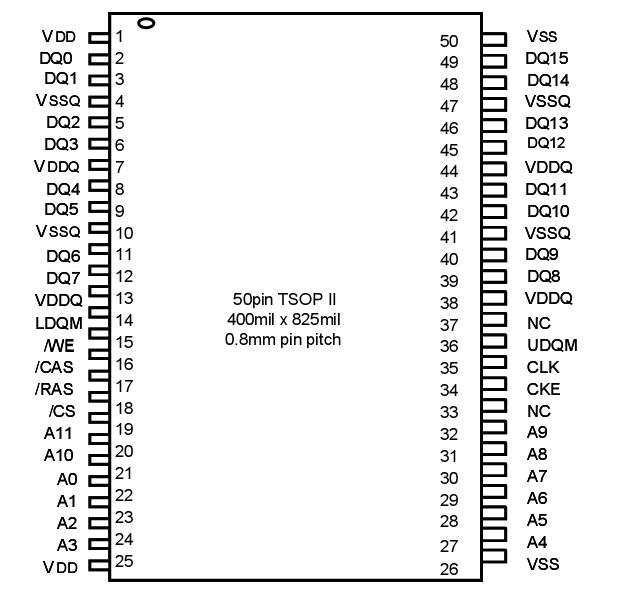 Specifications
| Parameter |
Symbol |
Rating |
Unit |
| Ambient Temperature |
TA |
0 ~ 70 |
°C |
| Storage Temperature |
TSTG |
-55 ~ 125 |
°C |
| Voltage on Any Pin relative to VSS |
VIN, VOUT |
-1.0 ~ 4.6 |
V |
| Voltage on VDD relative to VSS |
VDD |
-1.0 ~ 4.6 |
V |
| Short Circuit Output Current |
IOS |
50 |
mA |
| Power Dissipation |
PD |
1 |
W |
| Soldering Temperature·Time |
TSOLDER |
260·10 |
°C ·Sec |
DescriptionTHE Hynix HY57V161610E is a 16,777,216-bits CMOS Synchronous DRAM, ideally suited for the main memory and graphic appli- cations which require large memory density and high bandwidth. It is organized as 2banks of 524,288x16.
HY57V161610E is offering fully synchronous operation referenced to a positive edge clock. All inputs and outputs are synchronized with the rising edge of the clock input. The data paths are internally pipelined to achieve very high bandwidth. All input and output voltage levels are compatible with LVTTL.
HY57V161610E Programmable options include the length of pipeline (Read latency of 1,2 or 3), the number of consecutive read or write cycles initi- ated by a single control command (Burst length of 1,2,4,8 or full page), and the burst count sequence(sequential or interleave). A burst of read or write cycles in progress can be terminated by a burst terminate command or can be interrupted and replaced by a new burst read or write command on any cycle. (This pipeline design is not restricted by a `2N` rule.)

 HY57V161610E Data Sheet