HY57V281620HC(L/S)T-I

Features: •Single 3.3±0.3V power supply•All device pins are compatible with LVTTL interface•JEDEC standard 400mil 54pin TSOP-II with 0.8mm of pin pitch•All inputs and outputs referenced to positive edge of system clock•Data mask function by UDQM or LDQM•Internal...

product image

HY57V281620HC(L/S)T-I Picture
SeekIC No. : 004368236 Detail

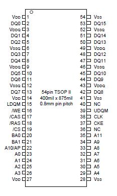
HY57V281620HC(L/S)T-I: Features: •Single 3.3±0.3V power supply•All device pins are compatible with LVTTL interface•JEDEC standard 400mil 54pin TSOP-II with 0.8mm of pin pitch•All inputs and outputs...

floor Price/Ceiling Price

Part Number:
HY57V281620HC(L/S)T-I
Supply Ability:
5000

Price Break

  • Qty
  • 1~5000
  • Unit Price
  • Negotiable
  • Processing time
  • 15 Days
Total Cost: $ 0.00

SeekIC Buyer Protection PLUS - newly updated for 2013!

  • Escrow Protection.
  • Guaranteed refunds.
  • Secure payments.
  • Learn more >>

Month Sales

268 Transactions

Rating

evaluate  (4.8 stars)

Upload time: 2024/5/2

Payment Methods

All payment methods are secure and covered by SeekIC Buyer Protection PLUS.

Notice: When you place an order, your payment is made to SeekIC and not to your seller. SeekIC only pays the seller after confirming you have received your order. We will also never share your payment details with your seller.
Product Details

Description


Features:

•Single 3.3±0.3V power supply
•All device pins are compatible with LVTTL interface
•JEDEC standard 400mil 54pin TSOP-II with 0.8mm of pin pitch
•All inputs and outputs referenced to positive edge of system clock
•Data mask function by UDQM or LDQM
•Internal four banks operation• Auto refresh and self refresh
•4096 refresh cycles / 64ms
•Programmable Burst Length and Burst Type - 1, 2, 4, 8 or Full page for Sequential Burst - 1, 2, 4 or 8 for Interleave Burst
•Programmable CAS Latency ; 2, 3 Clocks


Pinout

  Connection Diagram


Specifications

MAXIMUM RATINGS
Symbol
Rating
Unit
Ambient Temperature
TA
0 ~ 70
°C
Storage Temperature
TSTG
-55 ~ 125
°C
Voltage on Any Pin relative to VSS
VIN, VOUT
-1.0 ~ 4.6
V
Voltage on VDD relative to VSS
VDD, VDDQ
-1.0 ~ 4.6
V
Short Circuit Output Current
IOS
50
mA
Power Dissipation
PD
1
W
Soldering Temperature · Time
TSOLDER
260 · 10
°C · Sec


Description

The Hynix HY57V281620HC(L/S)T-I is a 134,217,728bit CMOS Synchronous DRAM, ideally suited for the Mobile applications which require low power consumption and extended temperature range. HY57V281620HC(L/S)T is organized as 4banks of 2,097,152x16

HY57V281620HC(L/S)T-I is offering fully synchronous operation referenced to a positive edge of the clock. All inputs and outputs are synchronized with the rising edge of the clock input. The data paths are internally pipelined to achieve very high bandwidth. All input and output voltage levels are compatible with LVTTL.


HY57V281620HC(L/S)T-I Programmable options include the length of pipeline (Read latency of 2 or 3), the number of consecutive read or write cycles initiated by a single control command (Burst length of 1,2,4,8, or full page), and the burst count sequence(sequential or interleave). A burst of read or write cycles in progress can be terminated by a burst terminate command or can be interrupted and replaced by a new burst read or write command on any cycle. (This pipelined design is not restricted by a `2N` rule.)


Customers Who Bought This Item Also Bought

Margin,quality,low-cost products with low minimum orders. Secure your online payments with SeekIC Buyer Protection.
Transformers
Boxes, Enclosures, Racks
Sensors, Transducers
Power Supplies - Board Mount
Audio Products
View more