HYB25D800T

Features: * Double data rate architecture: two data transfers per clock cycle* Bidirectional data strobe (DQS) is transmitted and received with data, to be used in capturing data at the receiver* DQS is edge-aligned with data for reads and is center-aligned with data for writes* Differential clock...

product image

HYB25D800T Picture
SeekIC No. : 004368839 Detail

HYB25D800T: Features: * Double data rate architecture: two data transfers per clock cycle* Bidirectional data strobe (DQS) is transmitted and received with data, to be used in capturing data at the receiver* DQ...

floor Price/Ceiling Price

Part Number:
HYB25D800T
Supply Ability:
5000

Price Break

  • Qty
  • 1~5000
  • Unit Price
  • Negotiable
  • Processing time
  • 15 Days
Total Cost: $ 0.00

SeekIC Buyer Protection PLUS - newly updated for 2013!

  • Escrow Protection.
  • Guaranteed refunds.
  • Secure payments.
  • Learn more >>

Month Sales

268 Transactions

Rating

evaluate  (4.8 stars)

Upload time: 2024/3/28

Payment Methods

All payment methods are secure and covered by SeekIC Buyer Protection PLUS.

Notice: When you place an order, your payment is made to SeekIC and not to your seller. SeekIC only pays the seller after confirming you have received your order. We will also never share your payment details with your seller.
Product Details

Description


Features:

* Double data rate architecture: two data transfers per clock cycle
* Bidirectional data strobe (DQS) is transmitted and received with data, to be used in capturing data at the receiver
* DQS is edge-aligned with data for reads and is center-aligned with data for writes
* Differential clock inputs (CK and CK)
* Four internal banks for concurrent operation
* Data mask (DM) for write data
* DLL aligns DQ and DQS transitions with CK transitions
* Commands entered on each positive CK edge; data and data mask referenced to both edges of DQS
* Burst Lengths: 2, 4, or 8
* CAS Latency: (1.5), 2, 2.5, (3)
* Auto Precharge option for each burst access
* Auto Refresh and Self Refresh Modes
* 7.8s Maximum Average Periodic Refresh Interval (8K refresh)
* 2.5V (SSTL_2 compatible) I/O
* VDDQ = 2.5V ± 0.2V / VDD = 2.5V ± 0.2V
* TSOP66 package
* 60 balls BGA w/ 3 depop rows ("chipsize package") 12 mm x 8 mm.


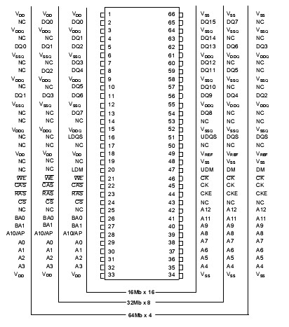
Pinout

  Connection Diagram


Specifications

Symbol Parameter
Rating
Units
VIN,VOUT Voltage on I/O pins relative to VSS
-0.5 to VDDQ +0.5
V
VIN Voltage on Inputs relative to VSS
-0.5 to +3.6
V
VDD Voltage on VDD supply relative to VSS
-0.5 to +3.6
V
VDDQ Voltage on VDDQ supply relative to VSS
-0.5 to +3.6
V
TA Operating Temperature (Ambient)
0 to 70
TSTG Storage Temperature (Plastic)
-55 to +150
PD Power Dissipation
1.0
W
IOUT Short Circuit Output Current
50
mA


Description

The 256Mb DDR SDRAM HYB25D800T is a high-speed CMOS, dynamic random-access memory containing 268,435,456 bits. It is internally configured as a quad-bank DRAM.


The 256Mb DDR SDRAM HYB25D800T uses a double-data-rate architecture to achieve high-speed operation. The double data rate architecture is essentially a 2n prefetch architecture with an interface designed to transfer two data words per clock cycle at the I/O pins. A single read or write access for the 256Mb DDR SDRAM effectively consists of a sinnal DRAM ore and two corresponding n-bit wide, onehalf-clock-cycle data transfers at the I/O pins.


A bidirectional data strobe (DQS) is transmitted externally, along with data, for use in data capture at the receiver. DQS is a strobe transmitted by the DDR SDRAM HYB25D800T during Reads and by the memory controller during Writes. DQS is edge-aligned with data for Reads and center-aligned with data for Writes.


The 256Mb DDR SDRAM HYB25D800T operates from a differential clock (CK and CK; the crossing of CK going HIGH and CK going LOW is referred to as the positive edge of CK). Commands (address and control signals) are registered at every positive edge of CK. Input data is registered on both edges of DQS, and output data is referenced to both edges of DQS, as well as to both edges of CK.


Read and write accesses to the DDR SDRAM HYB25D800T are burst oriented; accesses start at a selected location and continue for a programmed number of locations in a programmed sequence. Accesses begin with the registration of an Active command, which is then followed by a Read or Write command. The address bits registered coincident with the Active command are used to select the bank and row to be accessed. The address bits registered coincident with the Read or Write command are used to select the bank and the starting column location for the burst access.


The DDR SDRAM HYB25D800T provides for programmable Read or Write burst lengths of 2, 4 or 8 locations. An Auto Precharge function may be enabled to provide a self-timed row precharge that is initiated at the end of the burst access.

An auto refresh mode is provided along with a power-saving power-down mode. All inputs are compatible with the JEDEC Standard for SSTL_2. All outputs are SSTL_2, Class II compatible.


Customers Who Bought This Item Also Bought

Margin,quality,low-cost products with low minimum orders. Secure your online payments with SeekIC Buyer Protection.
Power Supplies - External/Internal (Off-Board)
Discrete Semiconductor Products
Tapes, Adhesives
803
Cables, Wires - Management
Potentiometers, Variable Resistors
View more