ICS2509C

Features: • Meets or exceeds PC133 registered DIMM specification 1.1• Spread Spectrum Clock Compatible• Distributes one clock input to one bank of five and one bank of four outputs• Separate output enable(OEA,OEB) for each output bank• Operating frequency 25 MHz to 17...

product image

ICS2509C Picture
SeekIC No. : 004370739 Detail

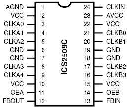
ICS2509C: Features: • Meets or exceeds PC133 registered DIMM specification 1.1• Spread Spectrum Clock Compatible• Distributes one clock input to one bank of five and one bank of four outputs...
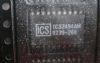
floor Price/Ceiling Price

Part Number:
ICS2509C
Supply Ability:
5000

Price Break

  • Qty
  • 1~5000
  • Unit Price
  • Negotiable
  • Processing time
  • 15 Days
Total Cost: $ 0.00

SeekIC Buyer Protection PLUS - newly updated for 2013!

  • Escrow Protection.
  • Guaranteed refunds.
  • Secure payments.
  • Learn more >>

Month Sales

268 Transactions

Rating

evaluate  (4.8 stars)

Upload time: 2025/12/26

Payment Methods

All payment methods are secure and covered by SeekIC Buyer Protection PLUS.

Notice: When you place an order, your payment is made to SeekIC and not to your seller. SeekIC only pays the seller after confirming you have received your order. We will also never share your payment details with your seller.
Product Details

Description


Features:

• Meets or exceeds PC133 registered DIMM specification 1.1
• Spread Spectrum Clock Compatible
• Distributes one clock input to one bank of five and one bank of four outputs
• Separate output enable(OEA,OEB) for each output bank
• Operating frequency 25 MHz to 175 Mhz
• External feedback input (FBIN) terminal is used to synchrionize the outputs to the clock input
• No external RC network required
• Operates at 3.3V Vcc
• Plastic 24-pin 173mil TSSOP package


Pinout

  Connection Diagram


Specifications

Supply Voltage (AVCC) .  . . . . . . AVCC < (Vcc + 0.7V)
Supply Voltage (VCC) . . . . . . . . . . . . . . . . . . . . 4.3 V
Logic Inputs . . . . . . . . . . . GND 0.5 V to Vcc +0.5 V
Ambient Operating Temperature .  . . . . 0 to +70
Storage Temperature . . .. . . . . . . . 65 to +150
Stresses above those listed under Absolute Maximum Ratings may cause permanent damage to the device. These ratings are stress specifications only and functional operation of the device at these or any other conditions above those listed in the operational sections of the specifications is not implied. Exposure to absolute maximum rating conditions for extended periods may affect product reliability.


Description

The ICS2509C is a high performance, low skew, low jitter clock driver. It uses a phase lock loop (PLL) technology to align, in both phase and frequency, the CLKIN signal with the CLKOUT signal. It is specifically designed for use with synchronous SDRAMs. The ICS2509C operates at 3.3V VCC and drives up to nine clock loads.

One bank of five outputs and one bank of four outputs of the ICS2509C provide nine low-skew, low-jitter copies of CLKIN. Output signal duty cycles are adjusted to 50 percent, independent of the duty cycle at CLKIN. Each bank of outputs can be enabled or disabled separately via control (OEA and OEB) inputs. When the OE inputs are high, the outputs align in phase and frequency with CLKIN; when the OE inputs are low, the outputs are disabled to the logic low state.

The ICS2509C does not require external RC filter components. The loop filter for the PLL is included on-chip, minimizing component count, board space, and cost. The buffer mode shuts off the PLL and connects the input directly to the output buffer. This buffer mode, the ICS2509C can be use as low skew fanout clock buffer device. The ICS2509C comes in 24 pin 173mil Thin Shrink Small-Outline package (TSSOP) package.


Customers Who Bought This Item Also Bought

Margin,quality,low-cost products with low minimum orders. Secure your online payments with SeekIC Buyer Protection.
Potentiometers, Variable Resistors
Semiconductor Modules
Soldering, Desoldering, Rework Products
Inductors, Coils, Chokes
Crystals and Oscillators
Memory Cards, Modules
View more