ICS8624

Features: * Fully integrated PLL* 5 differential HSTL outputs* Selectable differential CLKx, nCLKx input pairs* CLKx, nCLKx pairs can accept the following differential input levels: LVPECL, LVDS, HSTL, SSTL, HCSL* Output frequency range: 31.25MHz to 700MHz* Input frequency range: 31.25MHz to 700MH...

product image

ICS8624 Picture
SeekIC No. : 004371083 Detail

ICS8624: Features: * Fully integrated PLL* 5 differential HSTL outputs* Selectable differential CLKx, nCLKx input pairs* CLKx, nCLKx pairs can accept the following differential input levels: LVPECL, LVDS, HS...

floor Price/Ceiling Price

Part Number:
ICS8624
Supply Ability:
5000

Price Break

  • Qty
  • 1~5000
  • Unit Price
  • Negotiable
  • Processing time
  • 15 Days
Total Cost: $ 0.00

SeekIC Buyer Protection PLUS - newly updated for 2013!

  • Escrow Protection.
  • Guaranteed refunds.
  • Secure payments.
  • Learn more >>

Month Sales

268 Transactions

Rating

evaluate  (4.8 stars)

Upload time: 2025/12/4

Payment Methods

All payment methods are secure and covered by SeekIC Buyer Protection PLUS.

Notice: When you place an order, your payment is made to SeekIC and not to your seller. SeekIC only pays the seller after confirming you have received your order. We will also never share your payment details with your seller.
Product Details

Description


Features:

* Fully integrated PLL
* 5 differential HSTL outputs
* Selectable differential CLKx, nCLKx input pairs
* CLKx, nCLKx pairs can accept the following differential
     input levels:  LVPECL, LVDS, HSTL, SSTL, HCSL
* Output frequency range:  31.25MHz to 700MHz
* Input frequency range:  31.25MHz to 700MHz
* VCO range:  250MHz to 700MHz
* External feedback for "zero delay" clock regeneration
* Cycle-to-cycle jitter:  25ps (maximum)
* Output skew:  25ps (maximum)
* Static phase offset:  ±100ps
* 3.3V core, 1.8V output operating supply
* 0°C to 70°C ambient operating temperature
* Lead-Free package available
* Industrial temperature information available upon request


Application

As in any high speed analog circuitry, the power supply pins are vulnerable to random noise. The ICS8624 provides separate power supplies to isolate any high switching noise from the outputs to the internal PLL. VDD , V  DDA, and VDDO should be individually connected to the power supply plane through vias, and bypass capacitors should be
used for each pin. To achieve optimum jitter performance, power supply isolation is required. Figure 1 illustrates how a 10 resistor along with a 10F and a .01F bypass capacitor should be connected to each V DDApin.


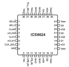
Pinout

  Connection Diagram


Specifications

Supply Voltage, V DD................................................4.6V
Inputs, ......................................VI -0.5V to V DD  + 0.5V
Outputs, I O
Continuous Current ...............................................50mA
  Surge Current ......................................................100mA
Package Thermal Impedance, JA .... 47.9°C/W (0 lfpm)
Storage Temperature, ..................TSTG -65°C to 150°C


Description

The ICS8624 is a high performance, 1-to-5 Differential-to-HSTL zero delay buffer and a member of the HiPerClockS(TM)   family of High Performance Clock Solutions from ICS. The ICS8624 has two selectable clock input pairs.

The CLK0, nCLK0 and CLK1, nCLK1 pair can accept most standard differential input levels. The VCO operates at a frequency range of 250MHz to 700MHz. Utilizing one of the outputs as feedback to the PLL, output frequencies up to 700MHz can be regenerated with zero delay with respect to the input. Dual reference clock inputs of the ICS8624 support redundant clock or multiple reference applications.


Customers Who Bought This Item Also Bought

Margin,quality,low-cost products with low minimum orders. Secure your online payments with SeekIC Buyer Protection.
Motors, Solenoids, Driver Boards/Modules
Cables, Wires - Management
RF and RFID
Circuit Protection
Integrated Circuits (ICs)
View more