Features: • 1 differential 3.3V LVPECL output pair, 1 differential feedback output pair
• Differential CLK, nCLK input pair
• CLK, nCLK pair can accept the following differential input levels: LVDS, LVPECL, LVHSTL, SSTL, HCSL
• Output frequency range: 31.25MHz to 700MHz
• Input frequency range: 31.25MHz to 700MHz
• VCO range: 250MHz to 700MHz
• Programmable dividers allow for the following output-to-input frequency ratios: 8:1, 4:1, 2:1, 1:1, 1:2, 1:4, 1:8
• External feedback for "zero delay" clock regeneration with configurable frequencies
• Cycle-to-cycle jitter: 25ps (maximum)
• Static phase offset: 50ps ± 100ps
• 3.3V supply voltage
• 0°C to 70°C ambient operating temperature
• Industrial temperature information available upon requestPinout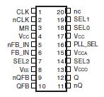 Specifications
Supply Voltage, VCC................................................................. 4.6V
Inputs, VI .........................................................-0.5V to VCC + 0.5V
Outputs, IO
Continuous Current ................................................................50mA
Surge Current....................................................................... 100mA
Package Thermal Impedance, JA ........................46.2°C/W (0 lfpm).
Storage Temperature, TSTG...................................... -65°C to 150°C
NOTE: Stresses beyond those listed under Absolute Maximum Ratings may cause permanent damage to the device. These ratings are stress specifications only. Functional operation of product at these conditions or any conditions beyond those listed in the DC Characteristics or AC Characteristics is not implied. Exposure to absolute maximum rating conditions for extended periods may affect product reliability.
DescriptionThe ICS8735-21 is a highly versatile 1:1 Differential-to-3.3V LVPECL clock generator and a member of the HiPerClockS™ family of High Performance Clock Solutions from ICS. The CLK, nCLK pair can accept most standard differential input levels. The ICS8735-21 has a fully integrated PLL and can be configured as zero delay buffer, multiplier or divider, and has an output frequency range of 31.25MHz to 700MHz. The reference divider, feedback divider and output divider are each programmable, thereby allowing for the following output-to-input frequency ratios: 8:1, 4:1, 2:1, 1:1, 1:2, 1:4, 1:8. The external feedback allows the device to achieve "zero delay" between the input clock and the output clocks. The PLL_SEL pin of the ICS8735-21 can be used to bypass the PLL for system test and debug purposes. In bypass mode, the reference clock is routed around the PLL and into the internal output dividers.

 ICS8735-21 Data Sheet